UM10375 All information provided in this document is subject to legal disclaimers. © NXP B.V. 2011. All rights reserved.
User manual Rev. 3 — 14 June 2011 293 of 368
NXP Semiconductors
UM10375
Chapter 16: LPC13xx 32-bit timer/counters (CT32B0/1)
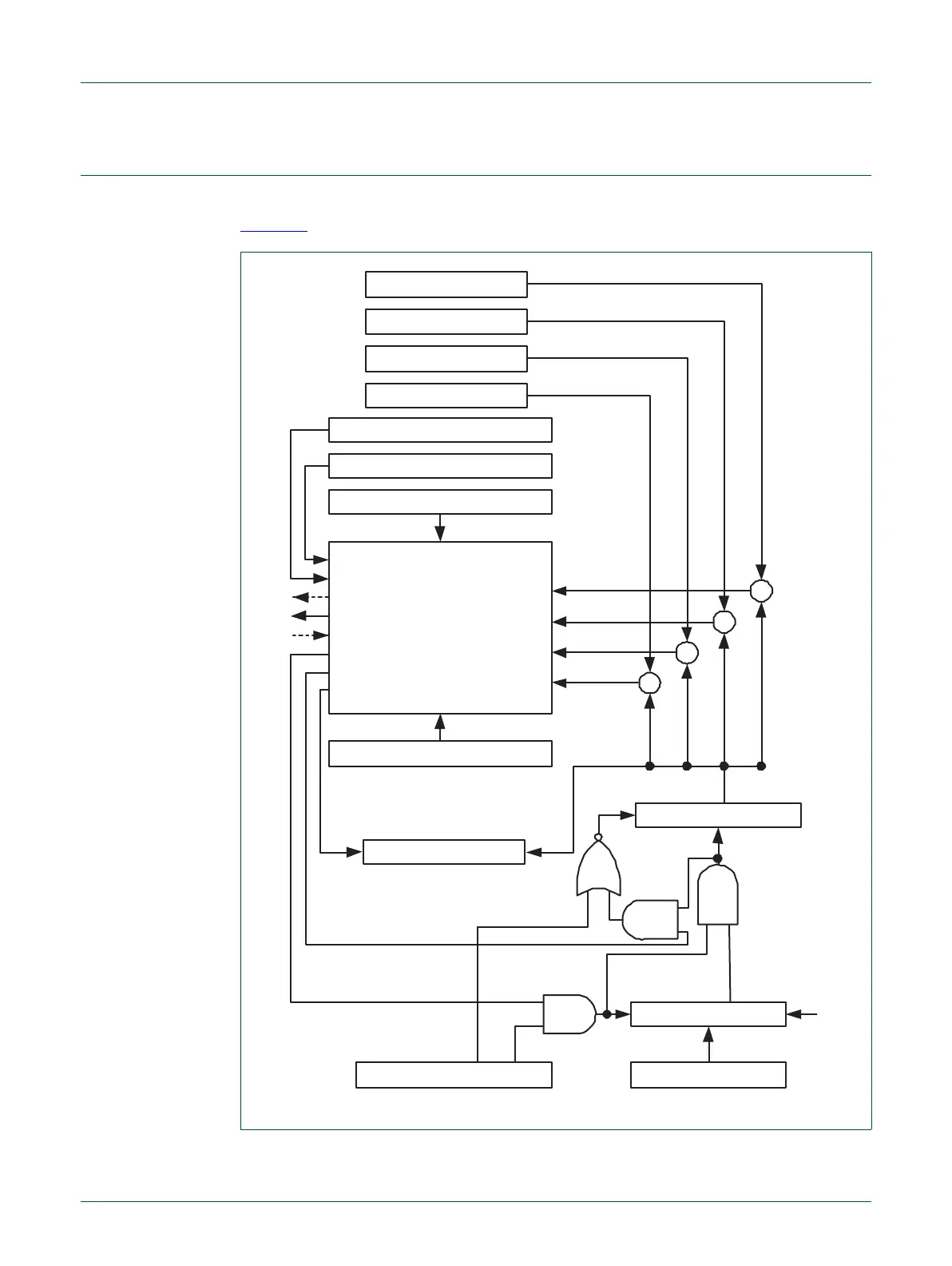
16.10 Architecture
The block diagram for 32-bit counter/timer0 and 32-bit counter/timer1 is shown in
Figure 56
.
Fig 56. 32-bit counter/timer block diagram
reset
MAXVAL
TIMER CONTROL REGISTER PRESCALE REGISTER
PRESCALE COUNTER
PCLK
enable
CAPTURE REGISTER 0
MATCH REGISTER 3
MATCH REGISTER 2
MATCH REGISTER 1
MATCH REGISTER 0
CAPTURE CONTROL REGISTER
CONTROL
TIMER COUNTER
CSN
TCI
CE
=
=
=
=
INTERRUPT REGISTER
EXTERNAL MATCH REGISTER
MATCH CONTROL REGISTER
MAT[3:0]
INTERRUPT
CAP0
STOP ON MATCH
RESET ON MATCH
LOAD[3:0]
 Loading...

