UM10375 All information provided in this document is subject to legal disclaimers. © NXP B.V. 2011. All rights reserved.
User manual Rev. 3 — 14 June 2011 7 of 368
NXP Semiconductors
UM10375
Chapter 1: LPC13xx Introductory information
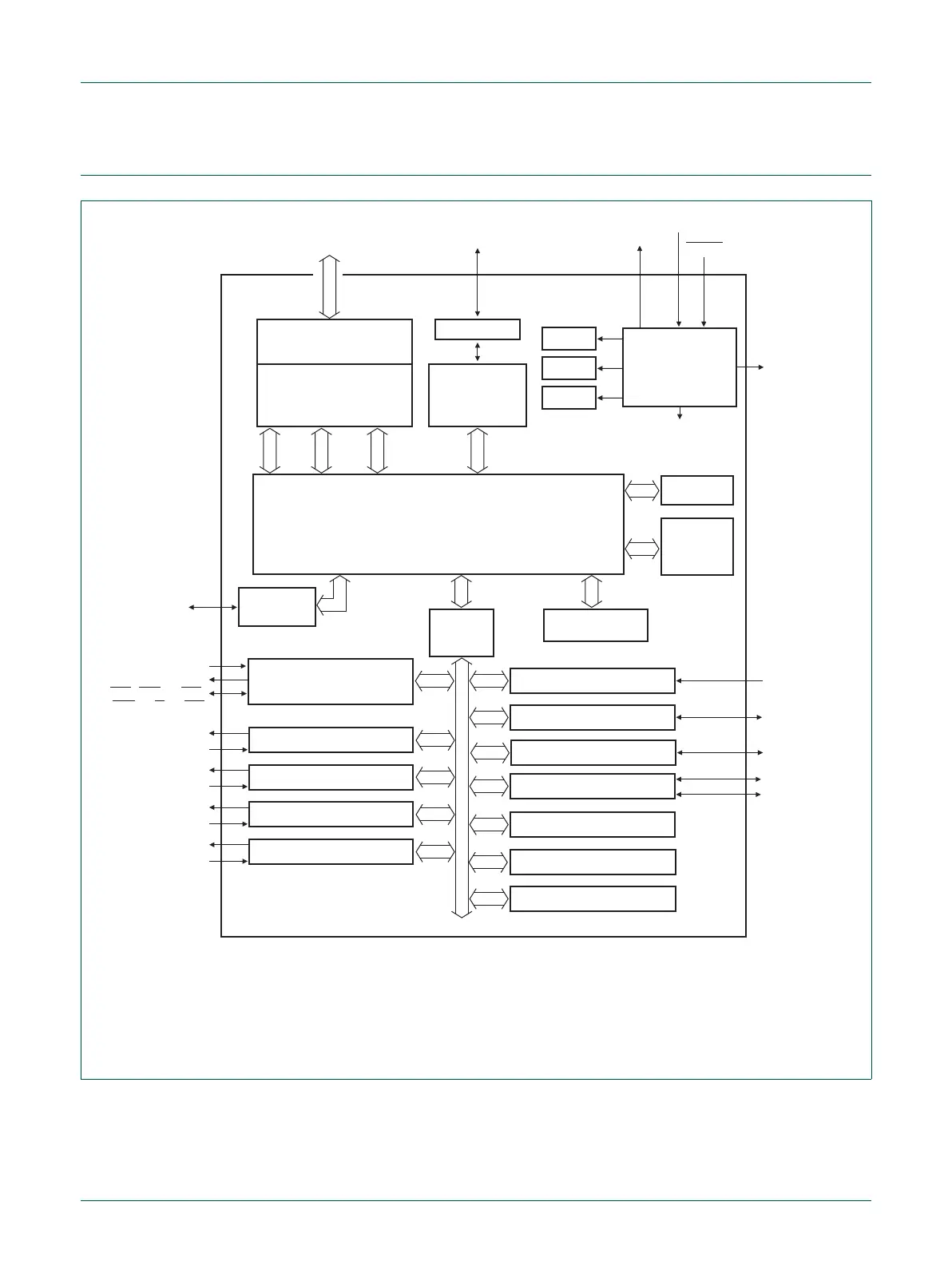
1.5 Block diagram
(1) LPC1342/43 only.
(2) LQFP48 package only.
(3) On LPC1313FBD48/01 only.
(4) Windowed WatchDog Timer (WWDT) on LPC1311/01 and LPC1313/01 only.
Fig 1. LPC13xx block diagram
SRAM
4/8 kB
ARM
CORTEX-M3
TEST/DEBUG
INTERFACE
FLASH
8/16/32 kB
USB DEVICE
CONTROLLER
(1)
I-code
bus
D-code
bus
system
bus
AHB TO
APB
BRIDGE
HIGH-SPEED
GPIO
CLOCK
GENERATION,
POWER CONTROL,
SYSTEM
FUNCTIONS
XTALIN
XTALOUT
RESET
clocks and
controls
SWD
USB PHY
(1)
SSP0
10-bit ADC
UART
32-bit COUNTER/TIMER 0
I
2
C-BUS
WDT/WWDT
(4)
IOCONFIG
LPC1311/13/42/43
slave
002aae722
slaveslave
slave
slave
ROM
slave
AHB-LITE BUS
GPIO ports
PIO0/1/2/3
CT32B0_MAT[3:0]
AD[7:0]
CT32B0_CAP0
SDA
SCL
RXD
TXD
DTR, DSR
(2)
, CTS,
DCD
(2)
, RI
(2)
, RTS
SYSTEM CONTROL
32-bit COUNTER/TIMER 1
CT32B1_MAT[3:0]
CT32B1_CAP0
16-bit COUNTER/TIMER 1
CT16B1_MAT[1:0]
CT16B1_CAP0
16-bit COUNTER/TIMER 0
CT16B0_MAT[2:0]
CT16B0_CAP0
USB pins
SCK0,SSEL0
MISO0, MOSI0
SSP1
(3)
SCK1,SSEL1
MISO1, MOSI0
CLKOUT
IRC
WDO
POR