UM10375 All information provided in this document is subject to legal disclaimers. © NXP B.V. 2011. All rights reserved.
User manual Rev. 3 — 14 June 2011 135 of 368
NXP Semiconductors
UM10375
Chapter 9: LPC13xx General Purpose I/O (GPIO)
9.5 Functional description
9.5.1 Write/read data operations
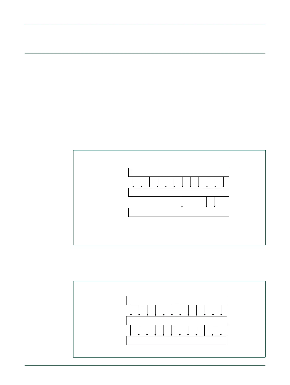
In order for software to be able to set GPIO bits without affecting any other pins in a single
write operation, bits [13:2] of a 14-bit wide address bus are used to create a 12-bit wide
mask for write and read operations on the 12 GPIO pins for each port. Only GPIODATA
bits masked by 1 are affected by read and write operations. The masked GPIODATA
register can be located anywhere between address offsets 0x0000 to 0x3FFC in the GPIO
address space. Reading and writing to the GPIODATA register at address 0x3FFC sets all
masking bits to 1.
Write operation
If the address bit (i+2) associated with the GPIO port bit i (i = 0 to 11) to be written is
HIGH, the value of the GPIODATA register bit i is updated. If the address bit (i+2) is LOW,
the corresponding GPIODATA register bit i is left unchanged.
Read operation
If the address bit associated with the GPIO data bit is HIGH, the value is read. If the
address bit is LOW, the GPIO data bit is read as 0: Reading a port DATA register yields
the state of port pins 11:0 ANDed with address bits 13:2.
Fig 14. Masked write operation to the GPIODATA register
Fig 15. Masked read operation
000000100110
111111100100
uuuuuu1uu10u
1312111098765432
00
ADDRESS[13:2]
address 0x098
data 0xFE4
GPIODATA register
at address + 0x098
u = unchanged
000000110001
111111100100
000000100000
1312111098765432
00
ADDRESS[13:2]
address 0x0C4
port pin settings
data read

 Loading...