AMCC Proprietary 205
Revision 1.02 - September 10, 2007
PPC405 Processor
dcbst
Data Cache Block Store
Preliminary User’s Manual
dcbst
Data Cache Block Store
EA ← (RA|0) + (RB)
DCBST(EA)
An effective address (EA) is formed by adding an index to a base address. The index is the contents of register RB.
The base address is 0 if the RA field is 0, and is the contents of register RA otherwise.
If the data block at the EA is in the data cache and marked as modified, the data block is copied back to main
storage and marked as unmodified in the data cache.
If the data block at the EA is in the data cache, and is not marked as modified, or if the data block at the EA is not
in the data cache, no operation is performed.
The operation specified by this instruction is performed whether or not the EA is marked as cacheable.
If instruction bit 31 contains 1, the contents of CR[CR0] are undefined.
Registers Altered
•None
Invalid Instruction Forms
• Reserved fields
Exceptions
This instruction is considered a “load” with respect to data storage exceptions. See Data Storage Interrupt on
page 120.
This instruction is considered a “store” with respect to data address compare (DAC) debug exceptions. See Debug
Interrupt on page 128.
Architecture Note
This instruction is part of the PowerPC Embedded Virtual Environment.
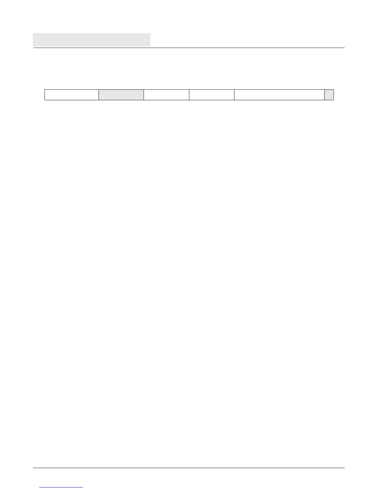
dcbst RA, RB
31
RA RB 54
0 6 11 16 21 31