AMCC Proprietary 206
Revision 1.02 - September 10, 2007
PPC405 Processor
dcbt
Data Cache Block Touch
Preliminary User’s Manual
dcbt
Data Cache Block Touch
EA ← (RA|0) + (RB)
DCBT(EA)
An effective address (EA) is formed by adding an index to a base address. The index is the contents of register RB.
The base address is 0 when the RA field is 0, and is the contents of register RA otherwise.
If the data block at the EA is not in the data cache and the EA is marked as cacheable, the block is read from main
storage into the data cache.
If the data block at the EA is in the data cache, or if the EA is marked as non cacheable, no operation is performed.
This instruction is not allowed to cause data storage exceptions or data TLB miss exceptions. If execution of the
instruction would cause such an exception, then no operation is performed, and no exception occurs.
If instruction bit 31 contains 1, the contents of CR[CR0] are undefined.
Registers Altered
•None
Invalid Instruction Forms
• Reserved fields
Programming Notes
The dcbt instruction allows a program to begin a cache block fetch from main storage before the program needs
the data. The program can later load data from the cache into registers without incurring the latency of a cache
miss.
Exceptions
This instruction is considered a “load” with respect to data storage exceptions. See Data Storage Interrupt on
page 120.
This instruction is considered a “load” with respect to data address compare (DAC) debug exceptions. See Debug
Interrupt on page 128.
Architecture Note
This instruction is part of the PowerPC Embedded Virtual Environment.
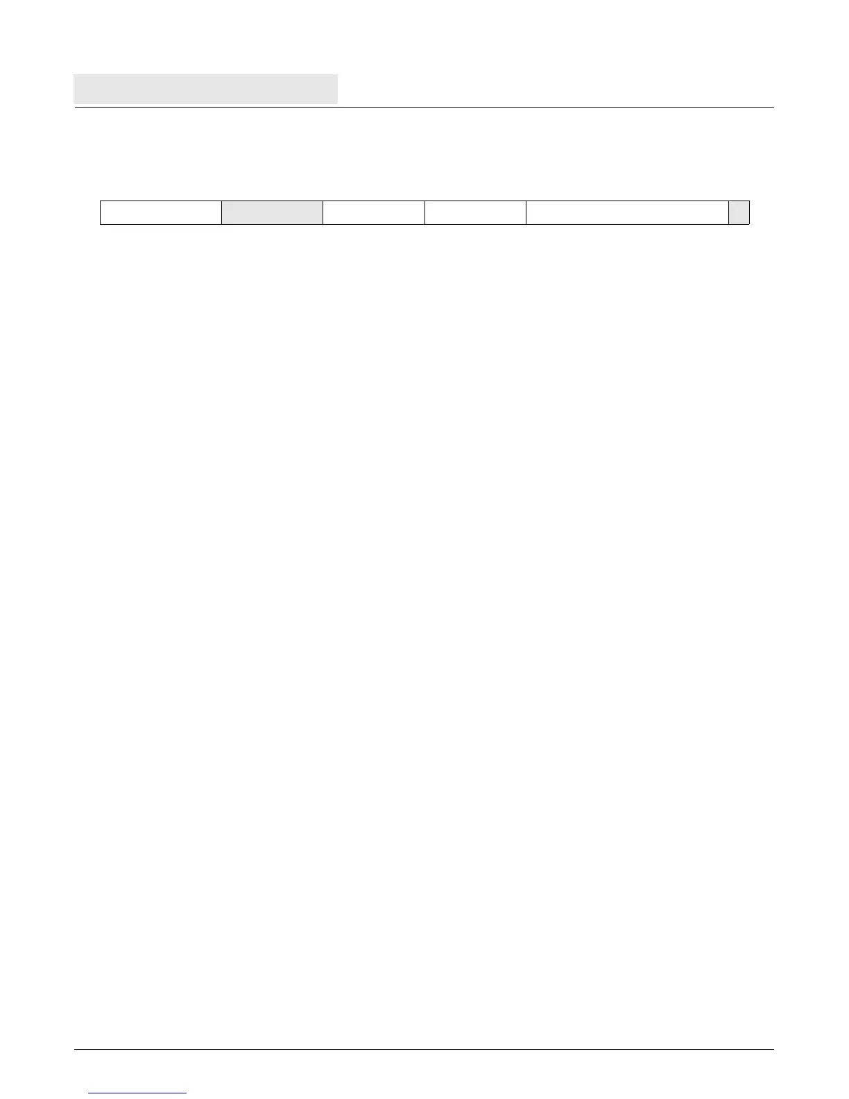
dcbt RA, RB
31
RA RB 278
0 6 11 16 21 31