AMCC Proprietary 211
Revision 1.02 - September 10, 2007
PPC405 Processor
dcread
Data Cache Read
Preliminary User’s Manual
dcread
Data Cache Read
EA ← (RA|0) + (RB)
if ((CCR0[CIS] = 0)
∧ (CCR0[CWS] = 0)) then (RT) ← (d-cache data, way A)
if ((CCR0[CIS] = 0)
∧ (CCR0[CWS] = 1)) then (RT) ← (d-cache data, way B)
if ((CCR0[CIS] = 1) ∧ (CCR0[CWS] = 0)) then (RT) ← (d-cache tag, way A)
if ((CCR0[CIS] = 1)
∧ (CCR0[CWS] = 1)) then (RT) ← (d-cache tag, way B)
An effective address (EA) is formed by adding an index to a base address. The index is the contents of register RB.
The base address is 0 if the RA field is 0 and is the contents of register RA otherwise.
This instruction is a debugging tool for reading the data cache entries for the congruence class specified by
EA
18:26
. The cache information is read into register RT.
If CCR0[CIS] = 0, the information is a word of data cache array data from the addressed congruence class. The
word is specified by EA
27:29
. If EA
30:31
are not 00, an alignment exception occurs. If CCR0[CWS] = 0, the data is
from the A-way; otherwise; the data is from the B-way.
If CCR0[CIS] = 1, the information is a cache tag from the addressed congruence class. If CCR0[CWS] = 0, the tag
is from the A-way; otherwise the tag is from the B-way.
Data cache tag information is placed into register RT as shown:
If instruction bit 31 contains 1, the contents of CR[CR0] are undefined.
Registers Altered
•RT
Invalid Instruction Forms
• Reserved fields
Programming Note
Execution of this instruction is privileged.
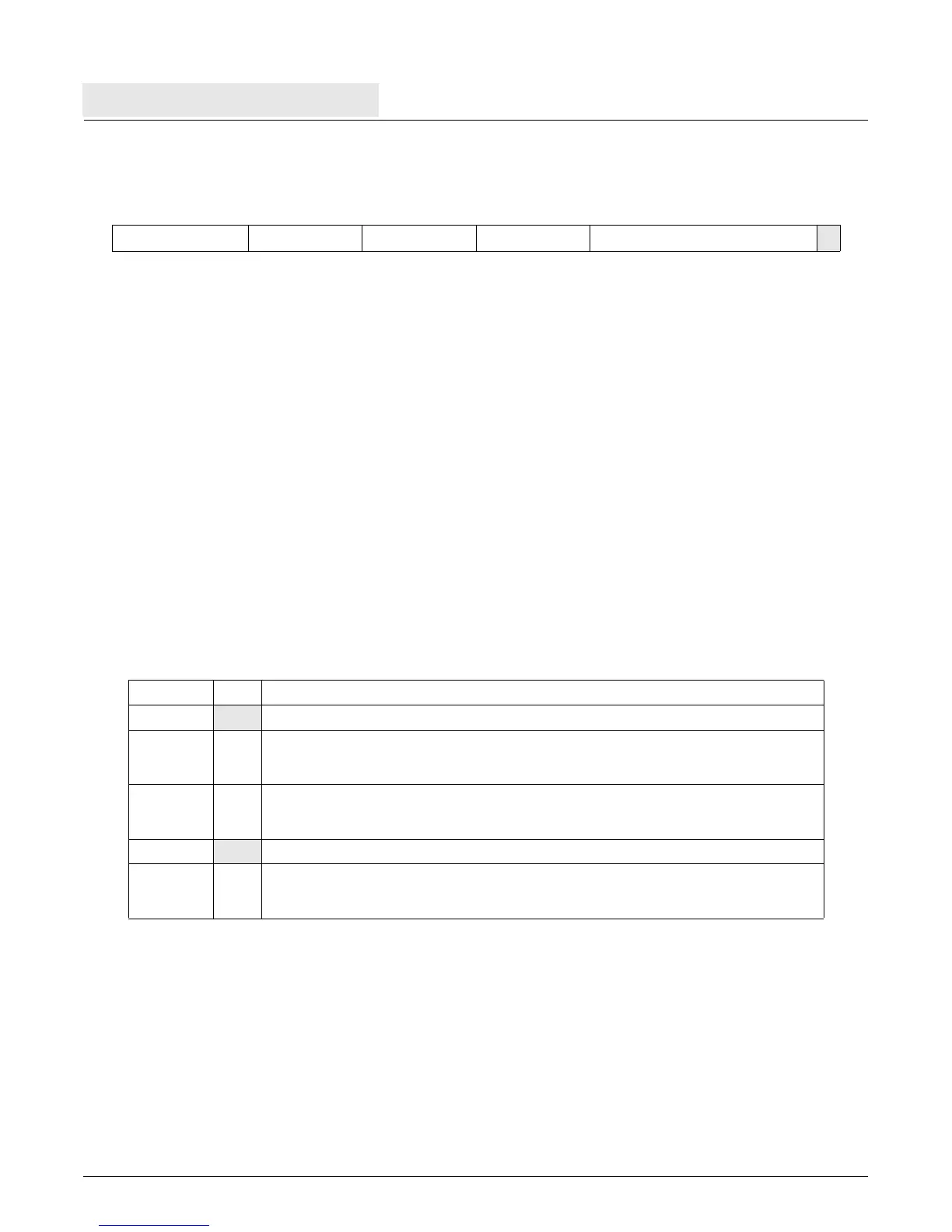
dcread RT, RA, RB
31 RT RA RB 486
0 6 11 16 21 31
0:19 TAG Cache Tag
20:25
Reserved
26 D
Cache Line Dirty
0 Not dirty
1Dirty
27 V
Cache Line Valid
0Not valid
1 Valid
28:30
Reserved
31 LRU
Least Recently Used (LRU)
0 A-way LRU
1 B-way LRU