Flexible static memory controller (FSMC) RM0033
1294/1381 RM0033 Rev 9
31.5.6 NOR/PSRAM control registers
The NOR/PSRAM control registers have to be accessed by words (32 bits).
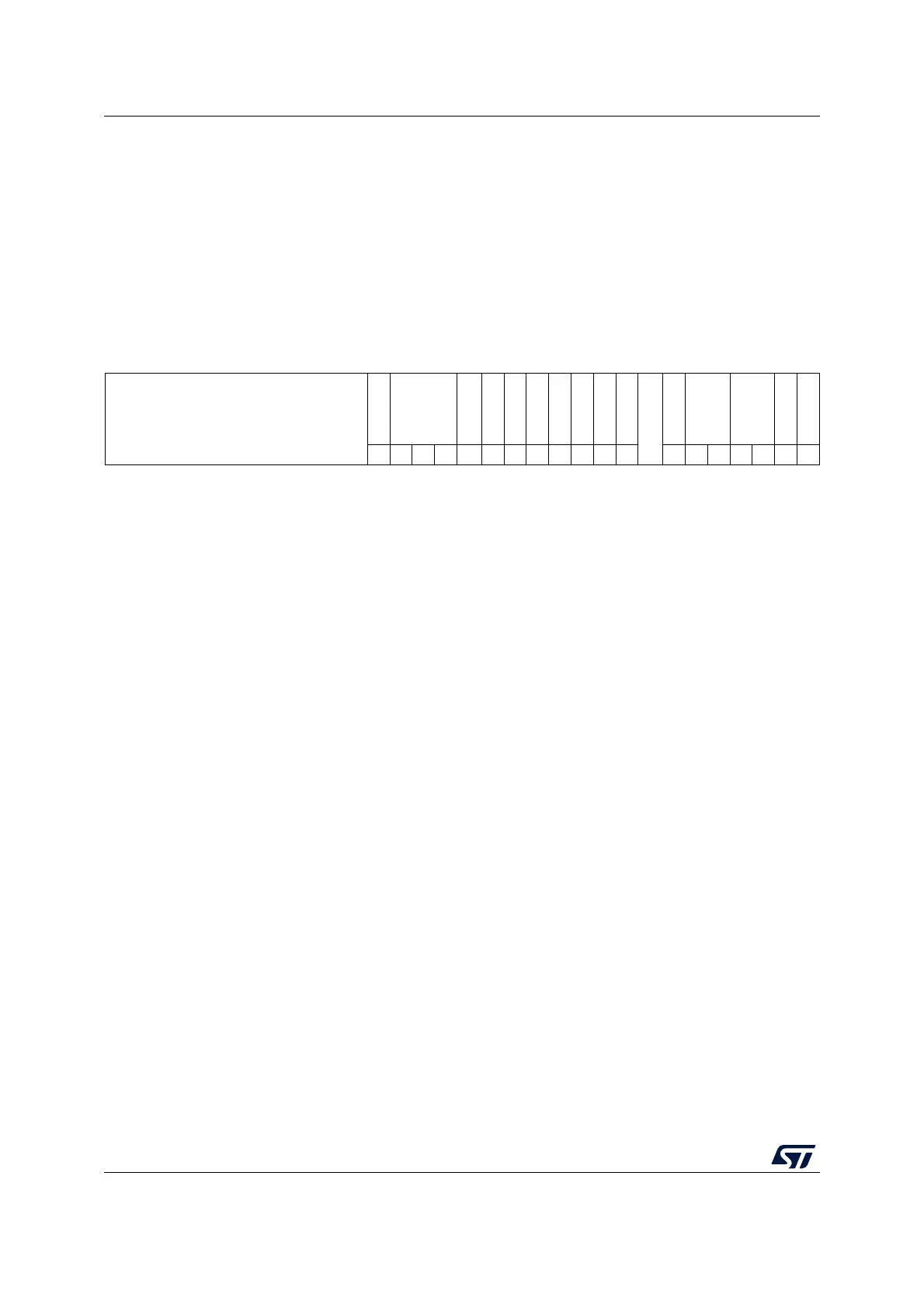
SRAM/NOR-Flash chip-select control registers 1..4 (FSMC_BCR1..4)
Address offset: 0xA000 0000 + 8 * (x – 1), x = 1...4
Reset value: 0x0000 30DB for Bank1 and 0x0000 30D2 for Bank 2 to 4
This register contains the control information of each memory bank, used for SRAMs,
PSRAM and NOR Flash memories.
3130292827262524232221201918171615141312111098 7 6543210
Reserved
CBURSTRW
CPSIZE[2:0]
ASCYCWAIT
EXTMOD
WAITEN
WREN
WAITCFG
WRAPMOD
WAITPOL
BURSTEN
Reserved
FACCEN
MWID[1:0]
MTYP[1:0]
MUXEN
MBKEN
rw rw rw rw rw rw rw rw rw rw rw rw rw rw rw rw
Bits 31: 20 Reserved, must be kept at reset value.
Bit 19 CBURSTRW: Write burst enable.
For Cellular RAM (PSRAM) memories, this bit enables the synchronous burst protocol
during write operations. The enable bit for synchronous read accesses is the BURSTEN
bit in the FSMC_BCRx register.
0: Write operations are always performed in asynchronous mode
1: Write operations are performed in synchronous mode.
Bits 18: 16
CPSIZE[2:0]: CRAM page size.
These are used for Cellular RAM 1.5 which does not allow burst access to cross the
address boundaries between pages. When these bits are configured, the FSMC
controller splits automatically the burst access when the memory page size is reached
(refer to memory datasheet for page size).
000: No burst split when crossing page boundary (default after reset)
001: 128 bytes
010: 256 bytes
011: 512 bytes
100: 1024 bytes
Others: reserved.
Bit 15 ASYNCWAIT: Wait signal during asynchronous transfers
This bit enables/disables the FSMC to use the wait signal even during an asynchronous
protocol.
0: NWAIT signal is not taken into account when running an asynchronous protocol
(default after reset)
1: NWAIT signal is taken into account when running an asynchronous protocol
 Loading...


