RM0033 Rev 9 717/1381
RM0033 Serial peripheral interface (SPI)
734
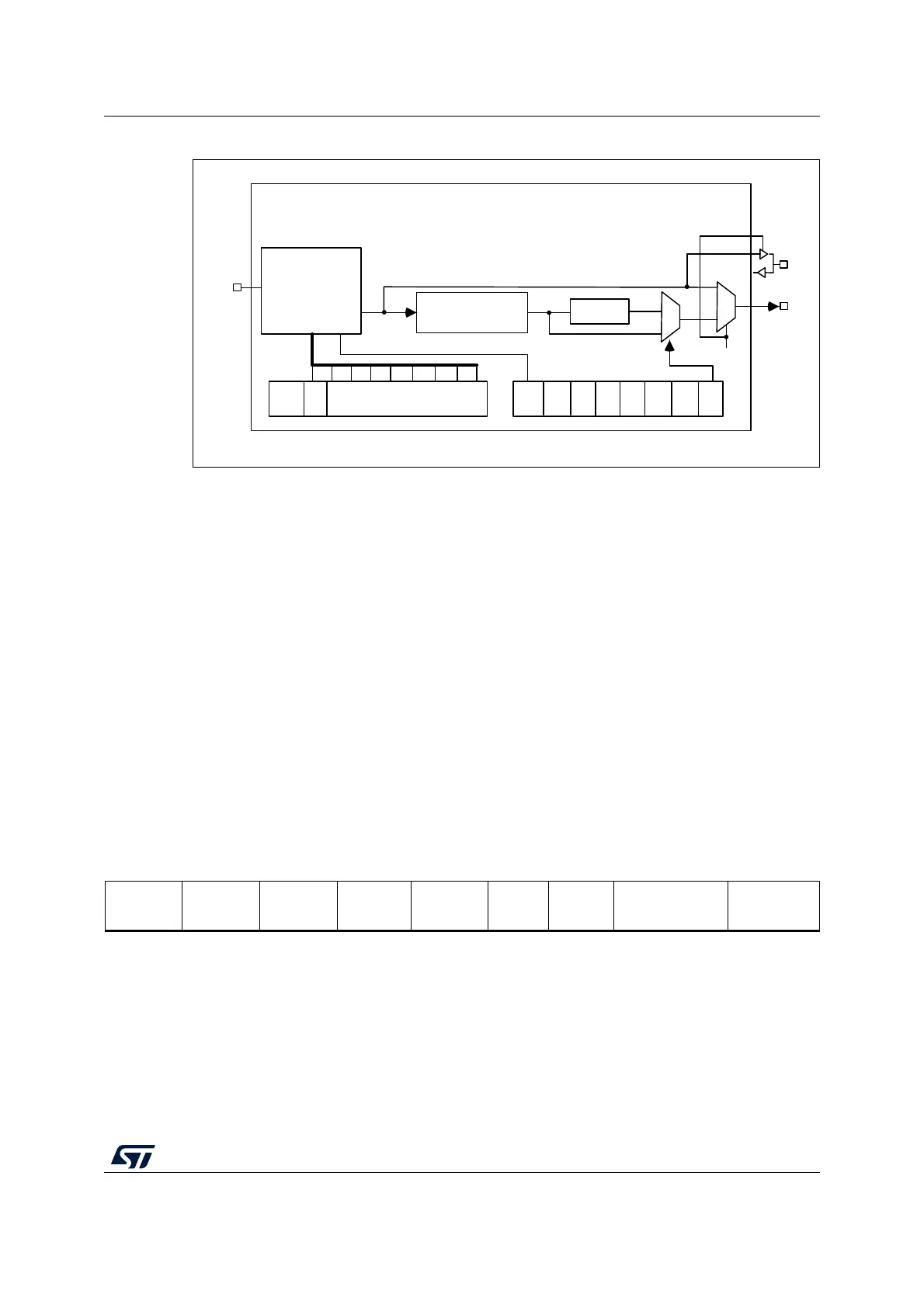
Figure 283. I
2
S clock generator architecture
1. Where x could be 2 or 3.
Figure 282 presents the communication clock architecture. To achieve high-quality audio
performance, the I2SxCLK clock source can be either the PLLI2S output (through R division
factor) or an external clock (mapped to I2S_CKIN pin).
The audio sampling frequency can be 96 kHz, 48 kHz, 44.1 kHz, 32 kHz, 22.05 kHz,
16 kHz, 11.025 kHz or 8 kHz (or any other value within this range). In order to reach the
desired frequency, the linear divider needs to be programmed according to the formulas
below:
When the master clock is generated (MCKOE in the SPI_I2SPR register is set):
F
S
= I2SxCLK / [(16*2)*((2*I2SDIV)+ODD)*8)] when the channel frame is 16-bit wide
F
S
= I2SxCLK / [(32*2)*((2*I2SDIV)+ODD)*4)] when the channel frame is 32-bit wide
When the master clock is disabled (MCKOE bit cleared):
F
S
= I2SxCLK / [(16*2)*((2*I2SDIV)+ODD))] when the channel frame is 16-bit wide
F
S
= I2SxCLK / [(32*2)*((2*I2SDIV)+ODD))] when the channel frame is 32-bit wide
Table 100 provides example precision values for different clock configurations.
Note: Other configurations are possible that allow optimum clock precision.
MS30109V1
MCKOE
ODD
8-bit linear divider
+ reshaping stage
Divider by 4
Div2
I²SDIV[7:0]
I²SMOD
CHLEN
0
1
0
1
MCKOE
CK
MCK
I²SxCLK
Table 100. Audio frequency precision (for PLLM VCO = 1 MHz or 2 MHz)
(1)
Master
clock
Target f
S
(Hz)
Data
format
PLLI2SN PLLI2SR I2SDIV I2SODD Real f
S
(Hz) Error
 Loading...


