RM0033 Rev 9 53/1381
RM0033 Memory and bus architecture
60
2.3.1 Embedded SRAM
The STM32F20x and STM32F21x feature 4 Kbytes of backup SRAM (see Section 4.1.2:
Battery backup domain) plus 128 Kbytes of system SRAM.
The system SRAM can be accessed as bytes, half-words (16 bits) or full words (32 bits).
The start address of the SRAM is 0x2000 0000. Read and write operations are performed at
CPU speed with 0 wait state.
The system SRAM is split up into two blocks, of 112 KB and 16 KB, with a capability for
concurrent access from by the AHB masters (like the Ethernet or the USB OTG HS): for
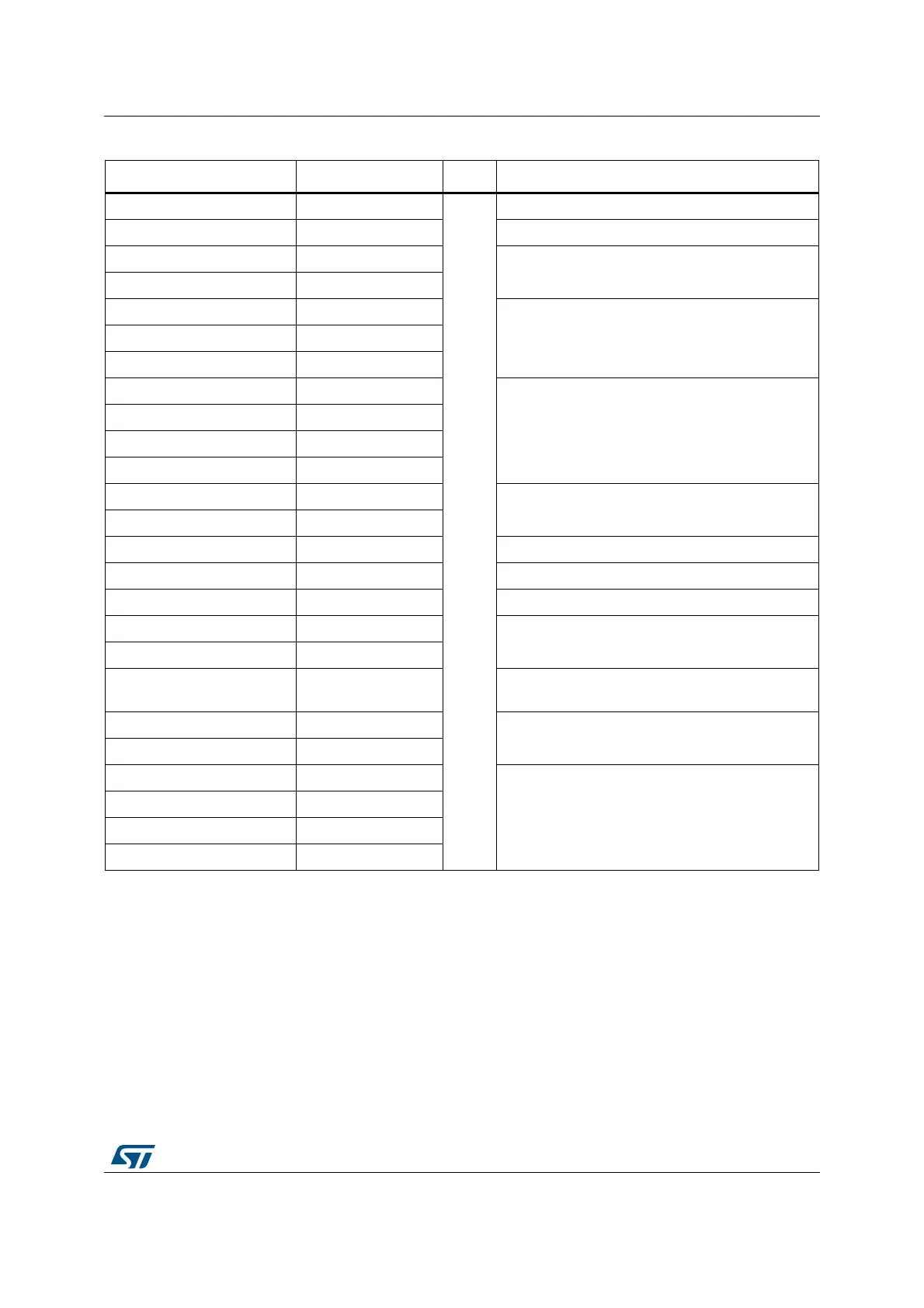
0x4000 7400 - 0x4000 77FF DAC
APB1
Section 11.5.15: DAC register map on page 276
0x4000 7000 - 0x4000 73FF PWR Section 4.4.3: PWR register map on page 83
0x4000 6800 - 0x4000 6BFF CAN2
Section 27.9.5: bxCAN register map on page 834
0x4000 6400 - 0x4000 67FF CAN1
0x4000 5C00 - 0x4000 5FFF I2C3
Section 23.6.10: I2C register map on page 6290x4000 5800 - 0x4000 5BFF I2C2
0x4000 5400 - 0x4000 57FF I2C1
0x4000 5000 - 0x4000 53FF UART5
Section 24.6.8: USART register map on page 681
0x4000 4C00 - 0x4000 4FFF UART4
0x4000 4800 - 0x4000 4BFF USART3
0x4000 4400 - 0x4000 47FF USART2
0x4000 3C00 - 0x4000 3FFF SPI3 / I2S3
Section 25.5.10: SPI register map on page 734
0x4000 3800 - 0x4000 3BFF SPI2 / I2S2
0x4000 3000 - 0x4000 33FF IWDG Section 17.4.5: IWDG register map on page 500
0x4000 2C00 - 0x4000 2FFF WWDG Section 18.6.4: WWDG register map on page 507
0x4000 2800 - 0x4000 2BFF RTC & BKP Registers Section 22.6.15: RTC register map on page 596
0x4000 2000 - 0x4000 23FF TIM14
Section 15.5.12: TIM10/11/13/14 register map on
page 482
0x4000 1C00 - 0x4000 1FFF TIM13
0x4000 1800 - 0x4000 1BFF TIM12
Section 15.4.14: TIM9/12 register map on
page 472
0x4000 1400 - 0x4000 17FF TIM7
Section 16.4.9: TIM6 and TIM7 register map on
page 495
0x4000 1000 - 0x4000 13FF TIM6
0x4000 0C00 - 0x4000 0FFF TIM5
Section 14.4.21: TIMx register map on page 435
0x4000 0800 - 0x4000 0BFF TIM4
0x4000 0400 - 0x4000 07FF TIM3
0x4000 0000 - 0x4000 03FF TIM2
Table 1. STM32F20x and STM32F21x register boundary addresses (continued)
Boundary address Peripheral Bus Register map
 Loading...


