Flexible static memory controller (FSMC) RM0033
1266/1381 RM0033 Rev 9
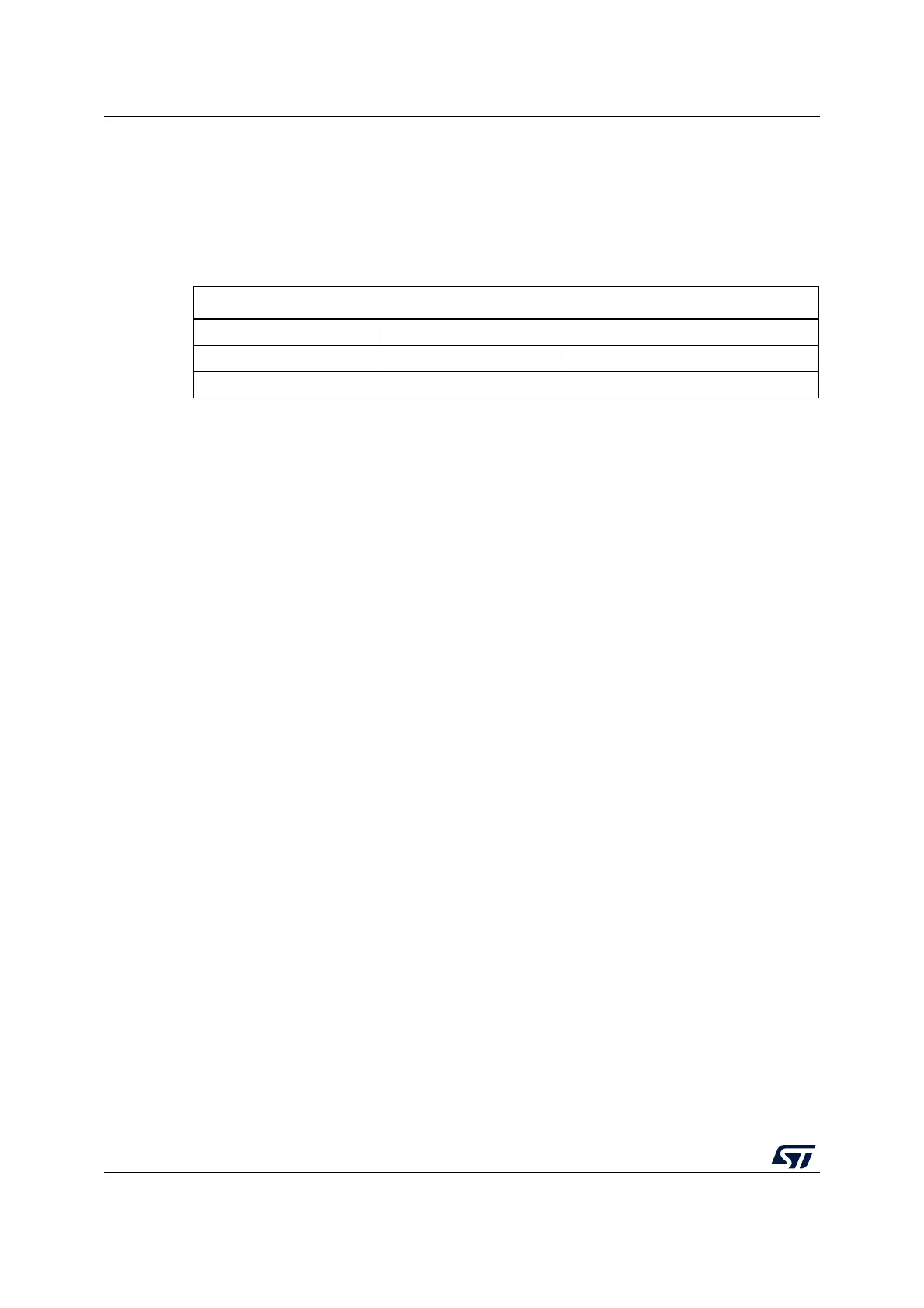
For NAND Flash memory, the common and attribute memory spaces are subdivided into
three sections (see in Table 172 below) located in the lower 256 Kbytes:
• Data section (first 64 Kbytes in the common/attribute memory space)
• Command section (second 64 Kbytes in the common / attribute memory space)
• Address section (next 128 Kbytes in the common / attribute memory space)
The application software uses the 3 sections to access the NAND Flash memory:
• To send a command to NAND Flash memory: the software must write the command
value to any memory location in the command section.
• To specify the NAND Flash address that must be read or written: the software
must write the address value to any memory location in the address section. Since an
address can be 4 or 5 bytes long (depending on the actual memory size), several
consecutive writes to the address section are needed to specify the full address.
• To read or write data: the software reads or writes the data value from or to any
memory location in the data section.
Since the NAND Flash memory automatically increments addresses, there is no need to
increment the address of the data section to access consecutive memory locations.
31.5 NOR Flash/PSRAM controller
The FSMC generates the appropriate signal timings to drive the following types of
memories:
• Asynchronous SRAM and ROM
–8-bit
– 16-bit
– 32-bit
• PSRAM (Cellular RAM)
– Asynchronous mode
– Burst mode for synchronous accesses
– Multiplexed or nonmultiplexed
• NOR Flash
– Asynchronous mode
– Burst mode for synchronous accesses
– Multiplexed or nonmultiplexed
The FSMC outputs a unique chip select signal NE[4:1] per bank. All the other signals
(addresses, data and control) are shared.
Table 172. NAND bank selections
Section name HADDR[17:16] Address range
Address section 1X 0x020000-0x03FFFF
Command section 01 0x010000-0x01FFFF
Data section 00 0x000000-0x0FFFF
 Loading...


