RM0033 Rev 9 55/1381
RM0033 Memory and bus architecture
60
2.3.3 Embedded Flash memory
The Flash memory has the following main features:
• Capacity up to 1 Mbyte
• 128 bits wide data read
• Byte, half-word, word and double word write
• Sector and mass erase
• Memory organization
The Flash memory is organized as follows:
– A main memory block divided into 4 sectors of 16 Kbytes, 1 sector of 64 Kbytes,
and 7 sectors of 128 Kbytes
– System memory from which the device boots in System memory boot mode
– 512 OTP (one-time programmable) bytes for user data
The OTP area contains 16 additional bytes used to lock the corresponding OTP
data block.
– Option bytes to configure read and write protection, BOR level, watchdog
software/hardware and reset when the device is in Standby or Stop mode
2.3.4 Flash memory read interface
Relation between CPU clock frequency and Flash memory read time
To correctly read data from Flash memory, the number of wait states (LATENCY) must be
correctly programmed in the Flash access control register (FLASH_ACR) according to the
frequency of the Cortex
®
-M3 clock and the supply voltage of the device. Table 3 shows the
correspondence between wait states and core clock frequency.
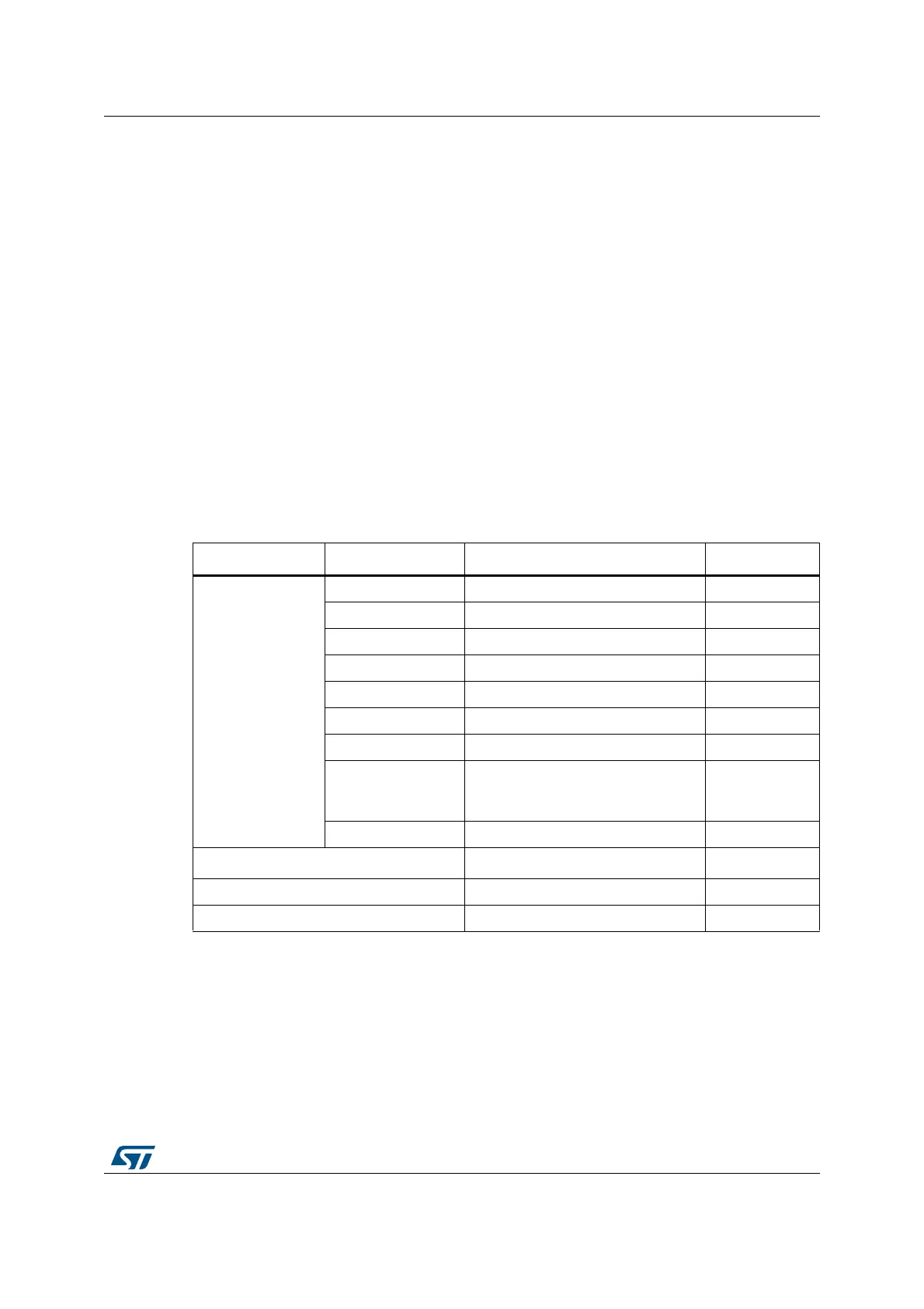
Table 2. Flash module organization
Block Name Block base addresses Size
Main memory
Sector 0 0x0800 0000 - 0x0800 3FFF 16 Kbyte
Sector 1 0x0800 4000 - 0x0800 7FFF 16 Kbyte
Sector 2 0x0800 8000 - 0x0800 BFFF 16 Kbyte
Sector 3 0x0800 C000 - 0x0800 FFFF 16 Kbyte
Sector 4 0x0801 0000 - 0x0801 FFFF 64 Kbyte
Sector 5 0x0802 0000 - 0x0803 FFFF 128 Kbyte
Sector 6 0x0804 0000 - 0x0805 FFFF 128 Kbyte
.
.
.
.
.
.
.
.
.
Sector 11 0x080E 0000 - 0x080F FFFF 128 Kbyte
System memory 0x1FFF 0000 - 0x1FFF 77FF 30 Kbyte
OTP 0x1FFF 7800 - 0x1FFF 7A0F 528 bytes
Option bytes 0x1FFF C000 - 0x1FFF C00F 16 bytes
 Loading...


