Advanced-control timers (TIM1 and TIM8) RM0033
366/1381 RM0033 Rev 9
Note: The state of the external I/O pins connected to the complementary OCx and OCxN channels
depends on the OCx and OCxN channel state and the GPIO registers.
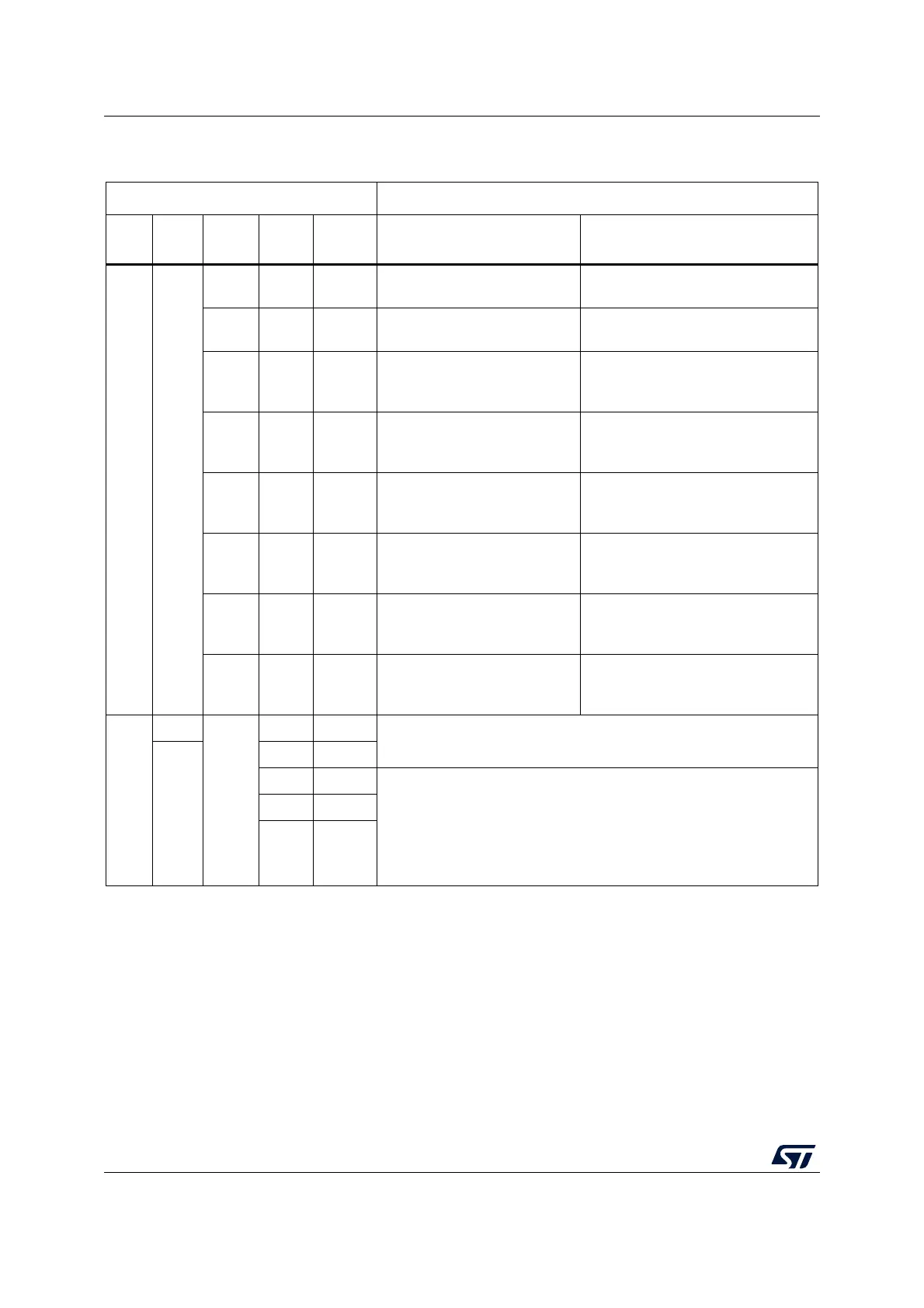
Table 57. Output control bits for complementary OCx and OCxN channels with
break feature
Control bits Output states
(1)
MOE
bit
OSSI
bit
OSSR
bit
CCxE
bit
CCxNE
bit
OCx output state OCxN output state
1X
00 0
Output Disabled (not driven by
the timer), OCx=0, OCx_EN=0
Output Disabled (not driven by the
timer), OCxN=0, OCxN_EN=0
00 1
Output Disabled (not driven by
the timer), OCx=0, OCx_EN=0
OCxREF + Polarity OCxN=OCxREF
xor CCxNP, OCxN_EN=1
01 0
OCxREF + Polarity
OCx=OCxREF xor CCxP,
OCx_EN=1
Output Disabled (not driven by the
timer)
OCxN=0, OCxN_EN=0
01 1
OCREF + Polarity + dead-time
OCx_EN=1
Complementary to OCREF (not
OCREF) + Polarity + dead-time
OCxN_EN=1
10 0
Output Disabled (not driven by
the timer)
OCx=CCxP, OCx_EN=0
Output Disabled (not driven by the
timer)
OCxN=CCxNP, OCxN_EN=0
10 1
Off-State (output enabled with
inactive state)
OCx=CCxP, OCx_EN=1
OCxREF + Polarity
OCxN=OCxREF xor CCxNP,
OCxN_EN=1
11 0
OCxREF + Polarity
OCx=OCxREF xor CCxP,
OCx_EN=1
Off-State (output enabled with
inactive state)
OCxN=CCxNP, OCxN_EN=1
11 1
OCREF + Polarity + dead-time
OCx_EN=1
Complementary to OCREF (not
OCREF) + Polarity + dead-time
OCxN_EN=1
0
0
X
XX
Output disabled (not driven by the timer anymore). The output state is
defined by the GPIO controller and can be High, Low or Hi-Z.
1
00
0 1 Off-State (output enabled with inactive state)
Asynchronously: OCx=CCxP, OCx_EN=1, OCxN=CCxNP,
OCxN_EN=1
Then if the clock is present: OCx=OISx and OCxN=OISxN after a
dead-time, assuming that OISx and OISxN do not correspond to OCX
and OCxN both in active state
10
11
1. When both outputs of a channel are not used (CCxE = CCxNE = 0), the OISx, OISxN, CCxP and CCxNP bits must be kept
cleared.