RM0033 Rev 9 347/1381
RM0033 Advanced-control timers (TIM1 and TIM8)
375
– CC1P=0 and CC1NP=’0’ in TIMx_CCER register to validate the polarity (and
detect rising edge only).
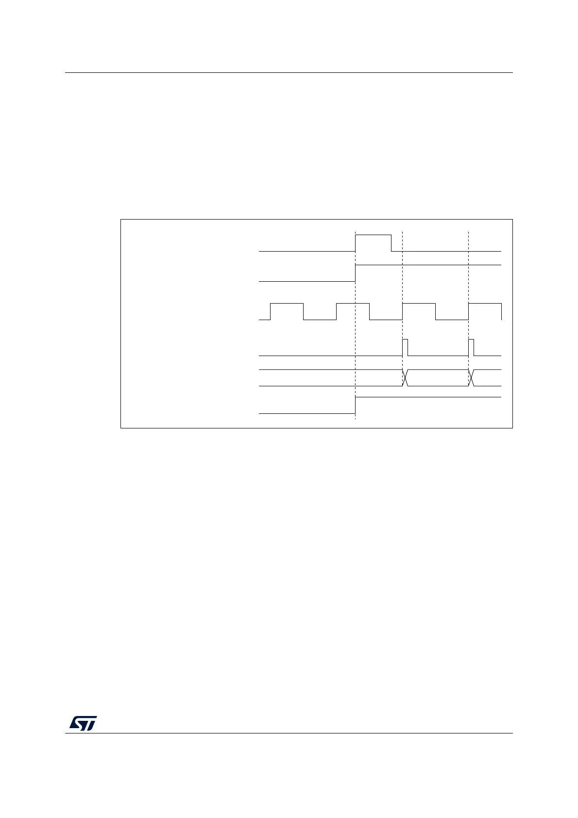
3. Configure the timer in trigger mode by writing SMS=110 in TIMx_SMCR register. Select
TI1 as the input source by writing TS=101 in TIMx_SMCR register.
A rising edge on TI1 enables the counter and sets the TIF flag. The counter then counts on
ETR rising edges.
The delay between the rising edge of the ETR signal and the actual reset of the counter is
due to the resynchronization circuit on ETRP input.
Figure 112. Control circuit in external clock mode 2 + trigger mode
13.3.20 Timer synchronization
The TIM timers are linked together internally for timer synchronization or chaining. Refer to
Section 14.3.15: Timer synchronization for details.
Note: The clock of the slave timer must be enabled prior to receive events from the master timer,
and must not be changed on-the-fly while triggers are received from the master timer.
13.3.21 Debug mode
When the microcontroller enters debug mode (Cortex
®
-M3 core halted), the TIMx counter
either continues to work normally or stops, depending on DBG_TIMx_STOP configuration
bit in DBG module. For more details, refer to Section 32.16.2: Debug support for timers,
watchdog, bxCAN and I
2
C.
For safety purposes, when the counter is stopped (DBG_TIMx_STOP = 1 in
DBGMCU_APBx_FZ register), the outputs are disabled (as if the MOE bit was reset). The
outputs can either be forced to an inactive state (OSSI bit = 1), or have their control taken
over by the GPIO controller (OSSI bit = 0) to force them to Hi-Z.
MS33110V1
34 35 36
TIF
Counter register
Counter clock = CK_CNT = CK_PSC
ETR
CEN/CNT_EN
TI1
 Loading...


