Secure digital input/output interface (SDIO) RM0033
780/1381 RM0033 Rev 9
26.9.6 SDIO response 1..4 register (SDIO_RESPx)
Address offset: (0x10 + (4 × x)); x = 1..4
Reset value: 0x0000 0000
The SDIO_RESP1/2/3/4 registers contain the status of a card, which is part of the received
response.
The Card Status size is 32 or 127 bits, depending on the response type.
The most significant bit of the card status is received first. The SDIO_RESP3 register LSB is
always 0b.
26.9.7 SDIO data timer register (SDIO_DTIMER)
Address offset: 0x24
Reset value: 0x0000 0000
The SDIO_DTIMER register contains the data timeout period, in card bus clock periods.
A counter loads the value from the SDIO_DTIMER register, and starts decrementing when
the data path state machine (DPSM) enters the Wait_R or Busy state. If the timer reaches 0
while the DPSM is in either of these states, the timeout status flag is set.
Note: A data transfer must be written to the data timer register and the data length register before
being written to the data control register.
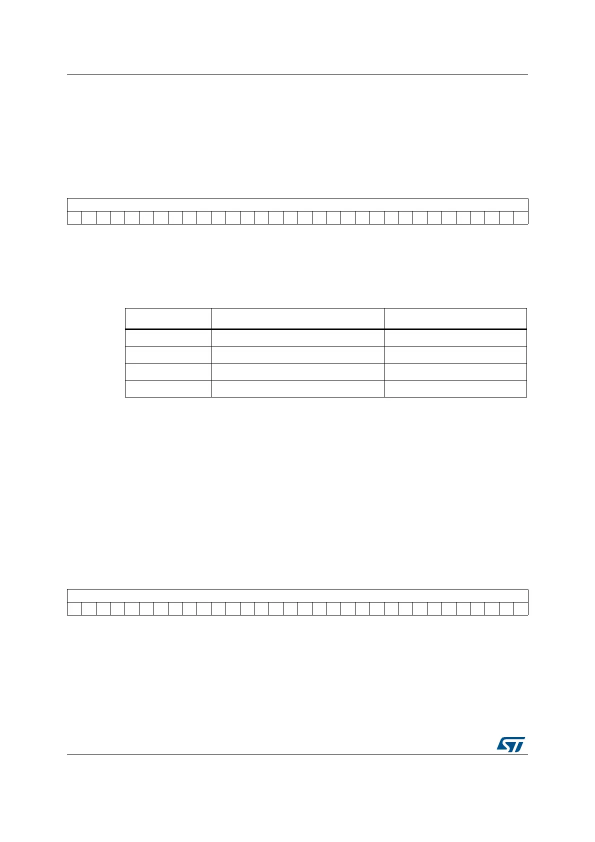
313029282726252423222120191817161514131211109876543210
CARDSTATUSx
rrrrrrrrrrrrrrrrrrrrrrrrrrrrrrrr
Bits 31:0 CARDSTATUSx: see Table 133.
Table 133. Response type and SDIO_RESPx registers
Register Short response Long response
SDIO_RESP1 Card Status[31:0] Card Status [127:96]
SDIO_RESP2 Unused Card Status [95:64]
SDIO_RESP3 Unused Card Status [63:32]
SDIO_RESP4 Unused Card Status [31:1]0b
313029282726252423222120191817161514131211109876543210
DATATIME
rw rw rw rw rw rw rw rw rw rw rw rw rw rw rw rw rw rw rw rw rw rw rw rw rw rw rw rw rw rw rw rw
Bits 31:0 DATATIME: Data timeout period
Data timeout period expressed in card bus clock periods.
 Loading...


