Inter-integrated circuit (I2C) interface RM0033
608/1381 RM0033 Rev 9
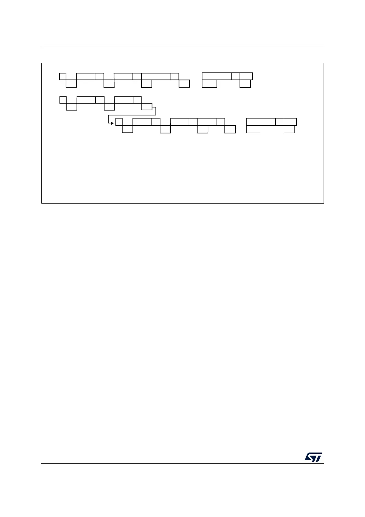
Figure 221. Transfer sequence diagram for master receiver
1. If a single byte is received, it is NA.
2. The EV5, EV6 and EV9 events stretch SCL low until the end of the corresponding software sequence.
3. The EV7 event stretches SCL low if the software sequence is not completed before the end of the next byte
reception.
4. The EV7_1 software sequence must be completed before the ACK pulse of the current byte transfer.
The procedures described below are recommended if the EV7-1 software sequence is not
completed before the ACK pulse of the current byte transfer.
These procedures must be followed to make sure:
• The ACK bit is set low on time before the end of the last data reception
• The STOP bit is set high after the last data reception without reception of
supplementary data.
For 2-byte reception:
• Wait until ADDR = 1 (SCL stretched low until the ADDR flag is cleared)
• Set ACK low, set POS high
• Clear ADDR flag
• Wait until BTF = 1 (Data 1 in DR, Data2 in shift register, SCL stretched low until a data
1 is read)
• Set STOP high
• Read data 1 and 2
7-bit master receiver
10-bit master receiver
Legend : S= Start, S
r
= Repeated Start, P= Stop, A= Acknowledge, NA= Non-acknowledge,
EVx= Event (with interrupt if ITEVFEN=1)
EV5: SB=1, cleared by reading SR1 register followed by writing DR register.
EV6: ADDR=1, cleared by reading SR1 register followed by reading SR2. In 10-bit master receiver mode, this se-
quence should be followed by writing CR2 with START = 1.
EV7: RxNE=1 cleared by reading DR register.
EV7_1: RxNE=1 cleared by reading DR register, program AC K=0 and STOP request
EV9: ADD10=1, cleared by reading SR1 register followed by writing DR register.
S Address A Data1 A
(1)
Data2 A
.....
DataN NA P
EV5 EV6 EV7 EV7 EV7_1 EV7
S Header A Address A
EV5 EV9 EV6
S
r
Header A
Data1 A
(1)
.....
EV5
EV6 EV7
Data2 A
EV7
DataN NA P
EV7_1 EV7
ai17540d
In case of the reception of 1 byte, the Acknowledge disable must be performed during EV6 event, i.e. before clearing ADDR flag.
 Loading...


