Flexible static memory controller (FSMC) RM0033
1264/1381 RM0033 Rev 9
Configuration registers
The FSMC can be configured using a register set. See Section 31.5.6, for a detailed
description of the NOR Flash/PSRAM control registers. See Section 31.6.8, for a detailed
description of the NAND Flash/PC Card registers.
31.4 External device address mapping
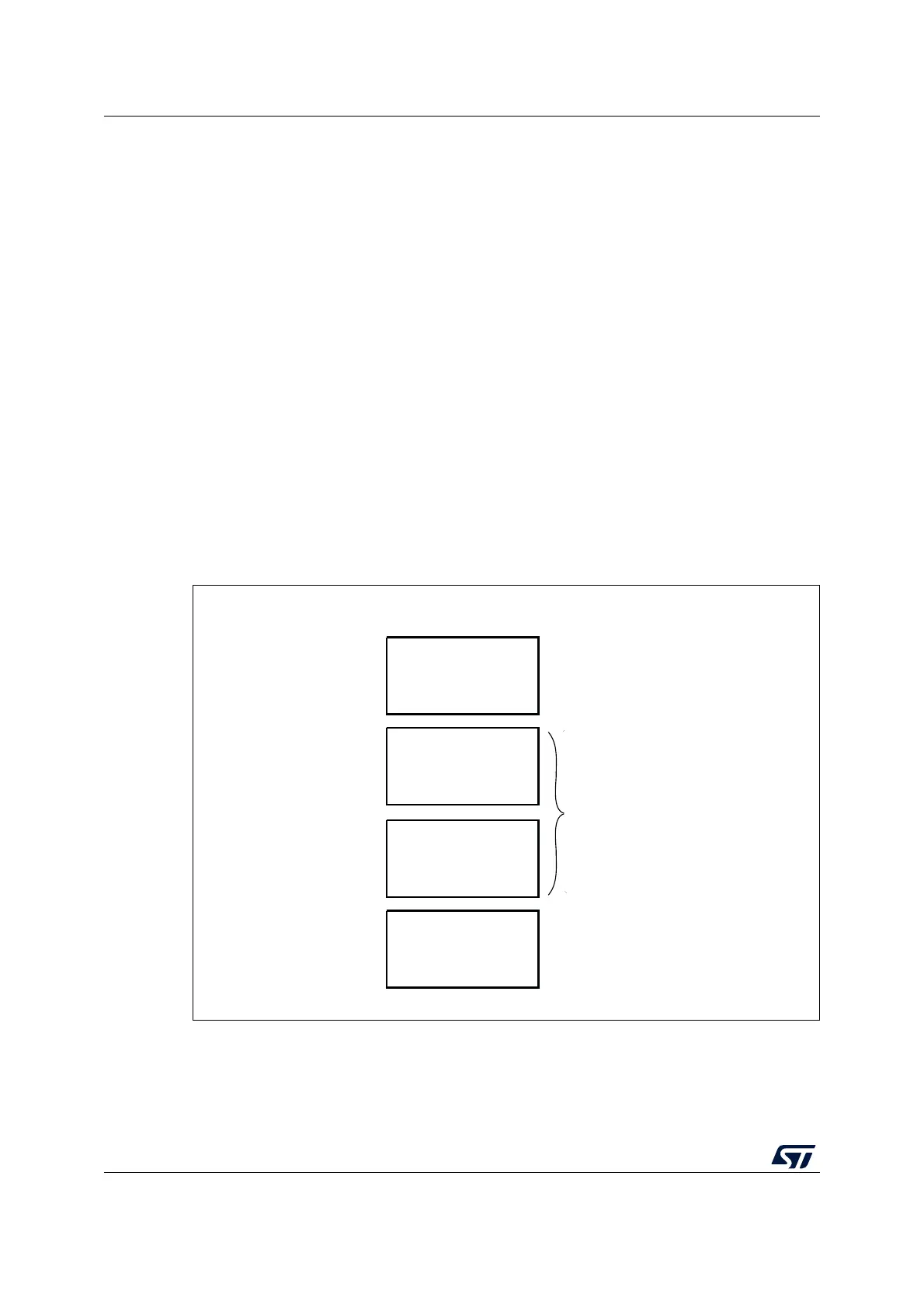
From the FSMC point of view, the external memory is divided into 4 fixed-size banks of
256 Mbytes each (Refer to Figure 398):
• Bank 1 used to address up to 4 NOR Flash or PSRAM memory devices. This bank is
split into 4 NOR/PSRAM subbanks with 4 dedicated Chip Selects, as follows:
– Bank 1 - NOR/PSRAM 1
– Bank 1 - NOR/PSRAM 2
– Bank 1 - NOR/PSRAM 3
– Bank 1 - NOR/PSRAM 4
• Banks 2 and 3 used to address NAND Flash devices (1 device per bank)
• Bank 4 used to address a PC Card device
For each bank the type of memory to be used is user-defined in the Configuration register.
Figure 398. FSMC memory banks
31.4.1 NOR/PSRAM address mapping
HADDR[27:26] bits are used to select one of the four memory banks as shown in Table 169.
Bank 1
NAND Flash
NOR / PSRAM
Supported memory typeBanks
4 × 64 MB
6000 0000h
6FFF FFFFh
Address
7000 0000h
7FFF FFFFh
8000 0000h
8FFF FFFFh
9000 0000h
9FFF FFFFh
Bank 2
4 × 64 MB
Bank 3
4 × 64 MB
Bank 4
4 × 64 MB
PC Card
ai14719
 Loading...


