Analog-to-digital converter (ADC) RM0033
250/1381 RM0033 Rev 9
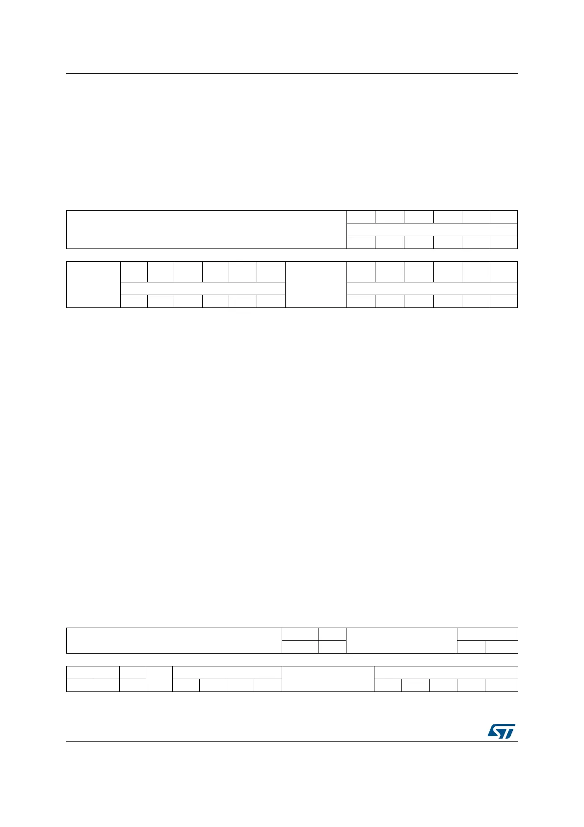
10.13.15 ADC Common status register (ADC_CSR)
Address offset: 0x00 (this offset address is relative to ADC1 base address + 0x300)
Reset value: 0x0000 0000
This register provides an image of the status bits of the different ADCs. Nevertheless it is
read-only and does not allow to clear the different status bits. Instead each status bit must
be cleared by writing it to 0 in the corresponding ADC_SR register.
10.13.16 ADC common control register (ADC_CCR)
Address offset: 0x04 (this offset address is relative to ADC1 base address + 0x300)
Reset value: 0x0000 0000
31 30 29 28 27 26 25 24 23 22 21 20 19 18 17 16
Reserved
OVR3 STRT3 JSTRT3 JEOC 3 EOC3 AWD3
ADC3
rrrrrr
15 14 13 12 11 10 9 8 7 6 5 4 3 2 1 0
Reserved
OVR2 STRT2
JSTRT
2
JEOC2 EOC2 AWD2
Reserved
OVR1 STRT1 JSTRT1 JEOC 1 EOC1 AWD1
ADC2 ADC1
rrrrrr r r r rrr
Bits 31:22 Reserved, must be kept at reset value.
Bits 7:6 Reserved, must be kept at reset value.
Bit 5 OVR1: Overrun flag of ADC1
This bit is a copy of the OVR bit in the ADC1_SR register.
Bit 4 STRT1: Regular channel Start flag of ADC1
This bit is a copy of the STRT bit in the ADC1_SR register.
Bit 3 JSTRT1: Injected channel Start flag of ADC1
This bit is a copy of the JSTRT bit in the ADC1_SR register.
Bit 2 JEOC1: Injected channel end of conversion of ADC1
This bit is a copy of the JEOC bit in the ADC1_SR register.
Bit 1 EOC1: End of conversion of ADC1
This bit is a copy of the EOC bit in the ADC1_SR register.
Bit 0 AWD1: Analog watchdog flag of ADC1
This bit is a copy of the AWD bit in the ADC1_SR register.
31 30 29 28 27 26 25 24 23 22 21 20 19 18 17 16
Reserved
TSVREFE VBATE
Reserved
ADCPRE
rw rw rw rw
15141312111098 7 654321 0
DMA[1:0] DDS
Res.
DELAY[3:0]
Reserved
MULTI[4:0]
rw rw rw rw rw rw rw rw rw rw rw rw
 Loading...


