RM0033 Rev 9 59/1381
RM0033 Memory and bus architecture
60
The values on the BOOT pins are latched on the 4th rising edge of SYSCLK after a reset. It
is up to the user to set the BOOT1 and BOOT0 pins after reset to select the required boot
mode.
BOOT0 is a dedicated pin while BOOT1 is shared with a GPIO pin. Once BOOT1 has been
sampled, the corresponding GPIO pin is free and can be used for other purposes.
The BOOT pins are also resampled when the device exits the Standby mode. Consequently,
they must be kept in the required Boot mode configuration when the device is in the Standby
mode. After this startup delay is over, the CPU fetches the top-of-stack value from address
0x0000 0000, then starts code execution from the boot memory starting from 0x0000 0004.
Note: When the device boots from SRAM, in the application initialization code, you have to
relocate the vector table in SRAM using the NVIC exception table and the offset register.
Physical remap
Once the boot pins are selected, the application software can modify the memory accessible
in the code area (in this way the code can be executed through the ICode bus in place of the
System bus). This modification is performed by programming the Section 7.2.1: SYSCFG
memory remap register (SYSCFG_MEMRMP) in the SYSCFG controller.
The following memories can thus be remapped:
• Main Flash memory
• System memory
• Embedded SRAM1 (112 KB)
• FSMC Bank 1 (NOR/PSRAM 1 and 2)
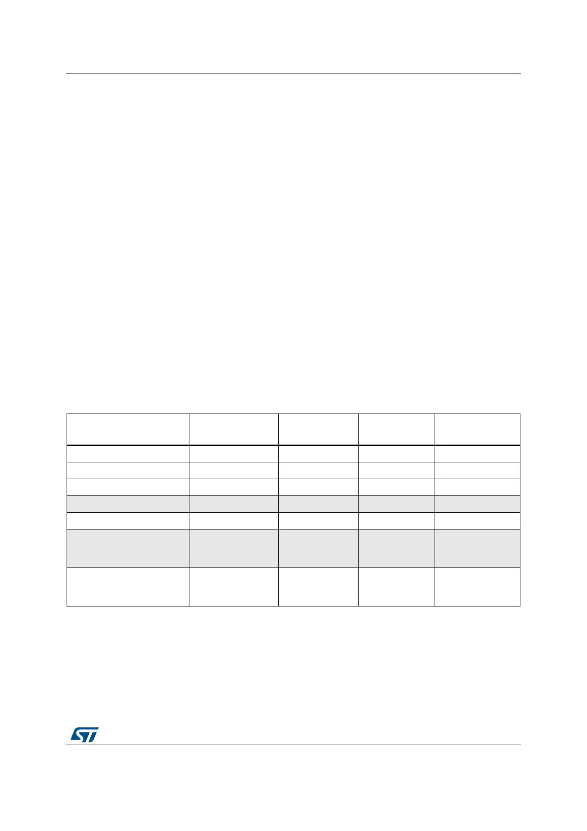
Table 5. Memory mapping vs. Boot mode/physical remap
Addresses
Boot/Remap in
main Flash memory
Boot/Remap in
embedded SRAM
Boot/Remap in
System memory
Remap in FSMC
0x2001 C000 - 0x2001 FFFF SRAM2 (16 KB) SRAM2 (16 KB) SRAM2 (16 KB) SRAM2 (16 KB)
0x2000 0000 - 0x2001 BFFF SRAM1 (112 KB) SRAM1 (112 KB) SRAM1 (112 KB) SRAM1 (112 KB)
0x1FFF 0000 - 0x1FFF 77FF System memory System memory System memory System memory
0x0810 0000 - 0x0FFF FFFF Reserved Reserved Reserved Reserved
0x0800 0000 - 0x080F FFFF Flash memory Flash memory Flash memory Flash memory
0x0400 0000 - 0x07FF FFFF Reserved Reserved Reserved
FSMC Bank1
NOR/PSRAM 2
(Aliased)
0x0000 0000 - 0x03FF
FFFF
(1)(2)
Flash (1 MB) Aliased
SRAM1 (112 KB)
Aliased
System memory
(30 KB) Aliased
FSMC Bank1
NOR/PSRAM 1
(Aliased)
1. When the FSMC is remapped at address 0x0000 0000, only the first two regions of Bank 1 memory controller (Bank1
NOR/PSRAM 1 and NOR/PSRAM 2) can be remapped. In remap mode, the CPU can access the external memory via
ICode bus instead of System bus which boosts up the performance. However, in remap mode, the FSMC addressing is
fixed to the remap address area only (Bank1 NOR/PSRAM 1 and NOR/PSRAM 2) and FSMC control registers are not
accessible. The FSMC remap function must be disabled to allows addressing other memory devices through the FSMC
and/or to access FSMC control registers.
2. Even when aliased in the boot memory space, the related memory is still accessible at its original memory space.
 Loading...


