DMA controller (DMA) RM0033
206/1381 RM0033 Rev 9
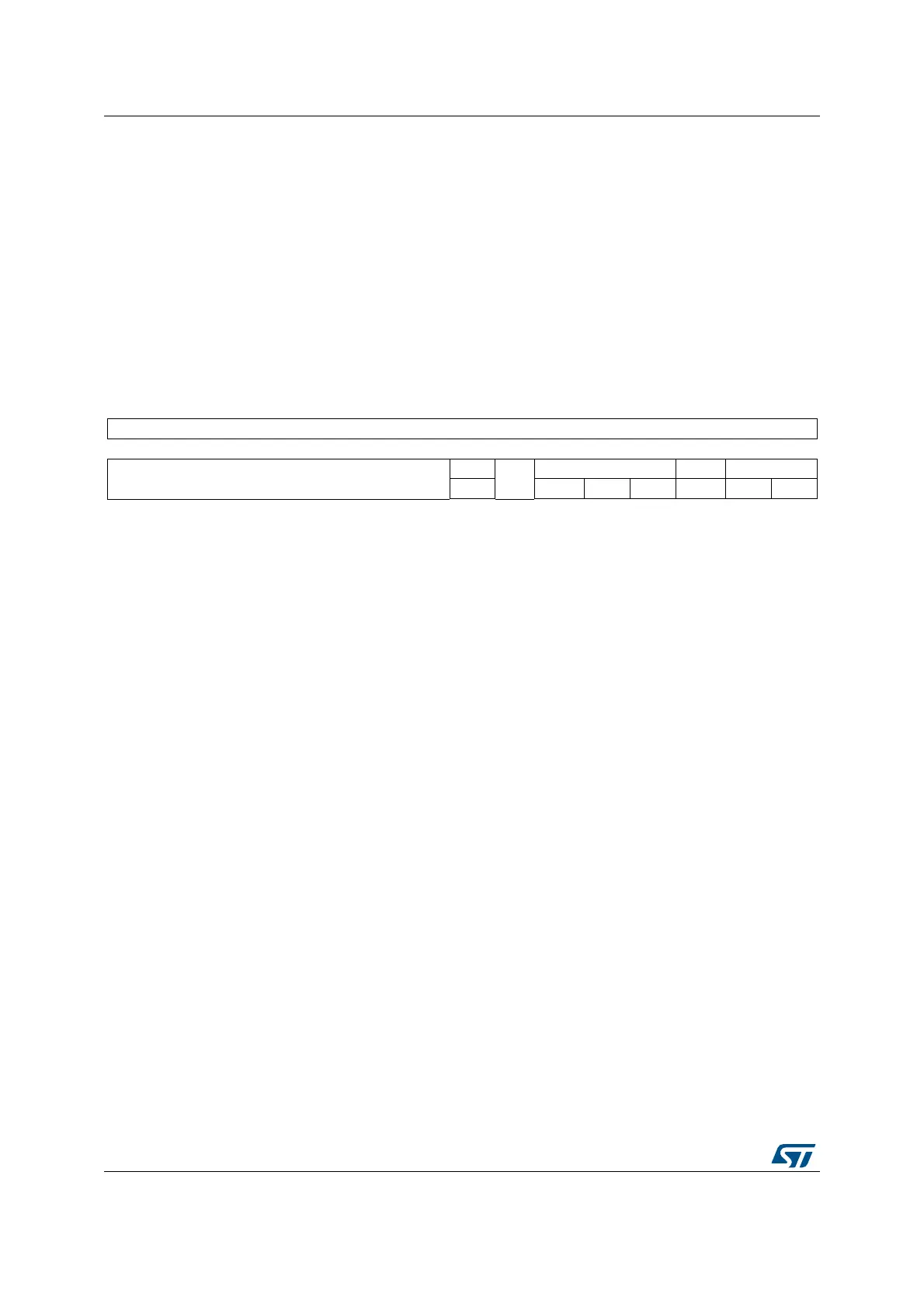
9.5.10 DMA stream x FIFO control register (DMA_SxFCR) (x = 0..7)
Address offset: 0x24 + 0x24 × stream number
Reset value: 0x0000 0021
Bits 31:0 M1A[31:0]: Memory 1 address (used in case of Double buffer mode)
Base address of Memory area 1 from/to which the data will be read/written.
This register is used only for the Double buffer mode.
These bits are write-protected. They can be written only if:
– the stream is disabled (bit EN= '0' in the DMA_SxCR register) or
– the stream is enabled (EN=’1’ in DMA_SxCR register) and bit CT = '0' in the
DMA_SxCR register.
31 30 29 28 27 26 25 24 23 22 21 20 19 18 17 16
Reserved
15 14 13 12 11 10 9 8 7 6 5 4 3 2 1 0
Reserved
FEIE
Reser
ved
FS[2:0] DMDIS FTH[1:0]
rw r r r rw rw rw
Bits 31:8 Reserved, must be kept at reset value.
Bit 7 FEIE: FIFO error interrupt enable
This bit is set and cleared by software.
0: FE interrupt disabled
1: FE interrupt enabled
Bit 6 Reserved, must be kept at reset value.
 Loading...


