Digital camera interface (DCMI) RM0033
290/1381 RM0033 Rev 9
12.7 DCMI interrupts
Five interrupts are generated. All interrupts are maskable by software. The global interrupt
(IT_DCMI) is the OR of all the individual interrupts. Table 53 gives the list of all interrupts.
12.8 DCMI register description
All DCMI registers have to be accessed as 32-bit words, otherwise a bus error occurs.
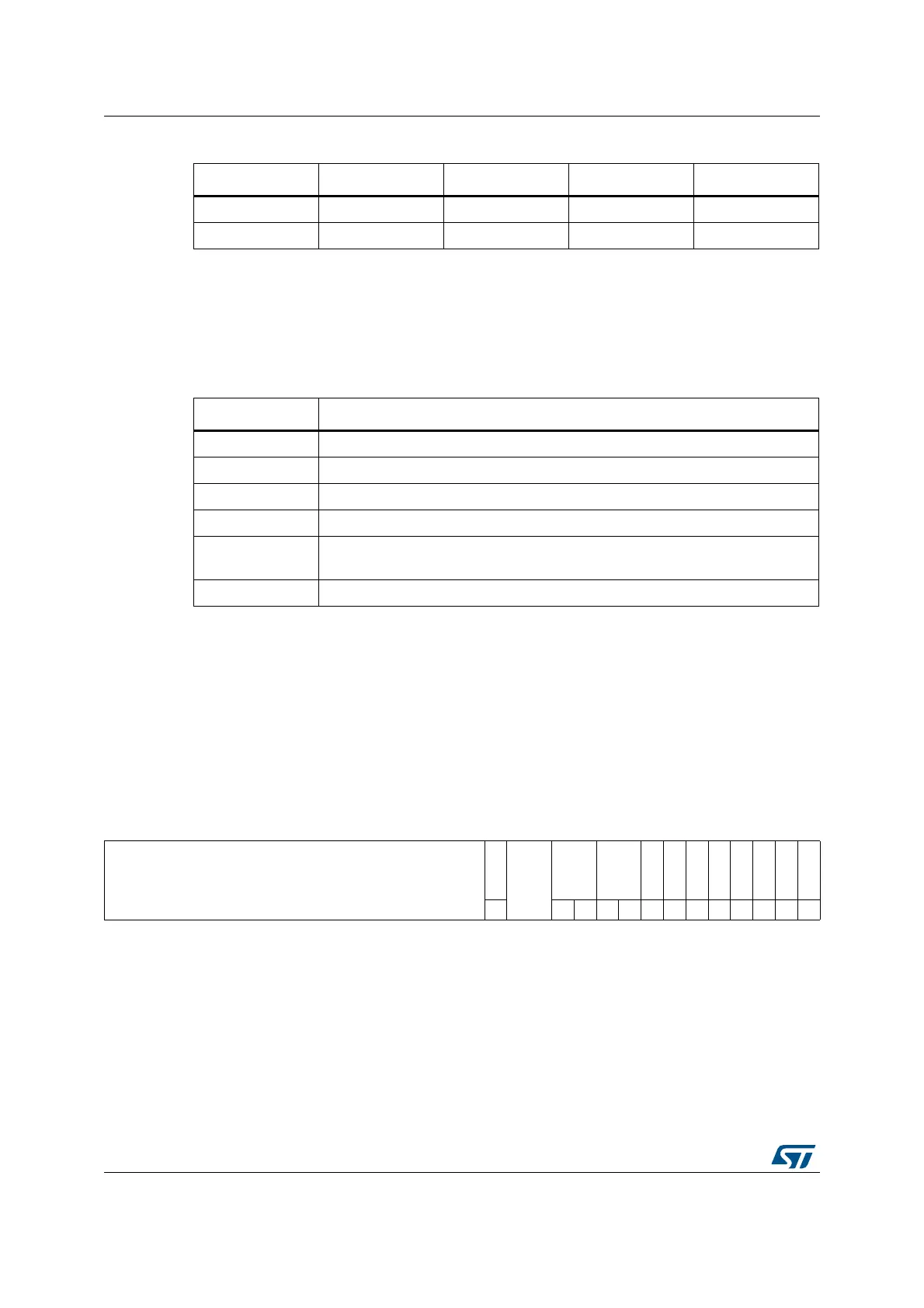
12.8.1 DCMI control register 1 (DCMI_CR)
Address offset: 0x00
Reset value: 0x0000 0x0000
Table 52. Data storage in YCbCr progressive video format
Byte address 31:24 23:16 15:8 7:0
0 Y n + 1 Cr n Y n Cb n
4 Y n + 3 Cr n + 2 Y n + 2 Cb n + 2
Table 53. DCMI interrupts
Interrupt name Interrupt event
IT_LINE Indicates the end of line
IT_FRAME Indicates the end of frame capture
IT_OVR indicates the overrun of data reception
IT_VSYNC Indicates the synchronization frame
IT_ERR
Indicates the detection of an error in the embedded synchronization frame
detection
IT_DCMI Logic OR of the previous interrupts
313029282726252423222120191817161514131211109876543210
Reserved
ENABLE
Reserved
EDM FCRC
VSPOL
HSPOL
PCKPOL
ESS
JPEG
CROP
CM
CAPTURE
rw rw rw rw rw rw rw rw rw rw rw rw rw
Bit 31:15 Reserved, must be kept at reset value.
Bit 14 ENABLE: DCMI enable
0: DCMI disabled
1: DCMI enabled
Note: The DCMI configuration registers should be programmed correctly before
enabling this Bit
Bit 13: 12 Reserved, must be kept at reset value.
 Loading...


