Secure digital input/output interface (SDIO) RM0033
738/1381 RM0033 Rev 9
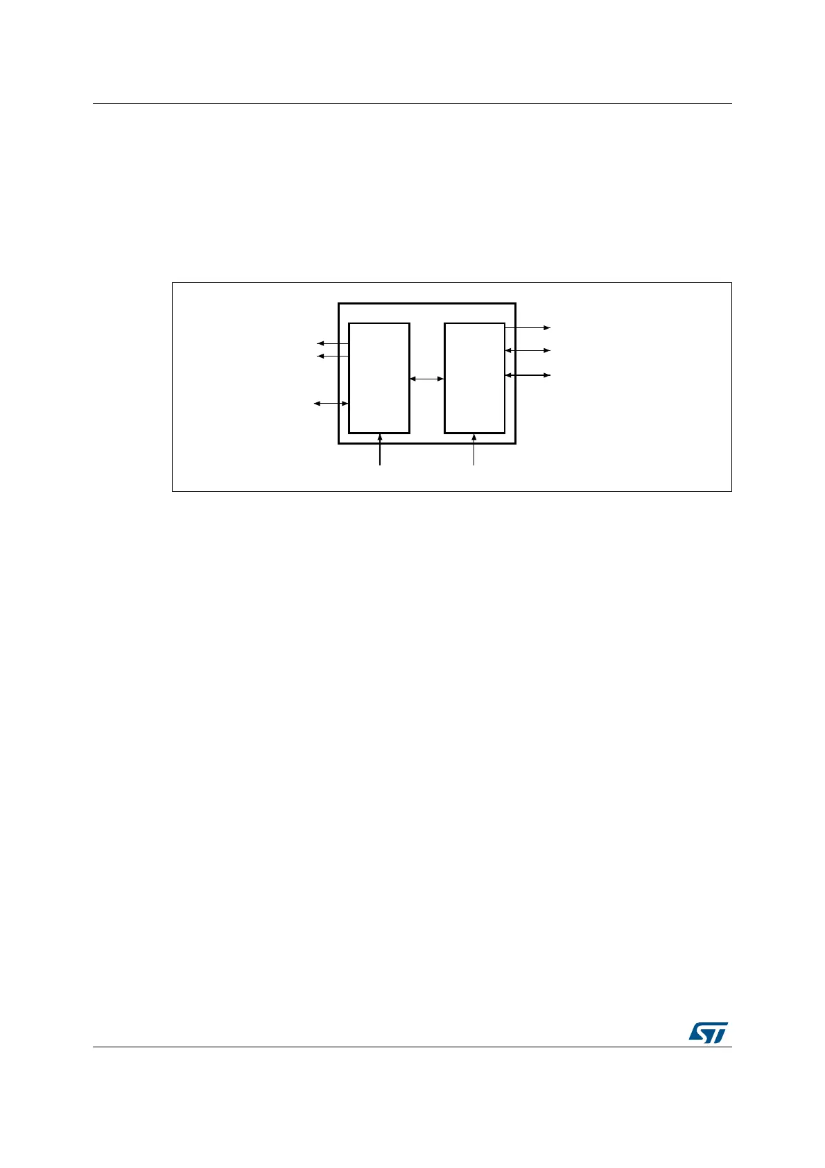
26.3 SDIO functional description
The SDIO consists of two parts:
• The SDIO adapter block provides all functions specific to the MMC/SD/SD I/O card
such as the clock generation unit, command and data transfer.
• The APB2 interface accesses the SDIO adapter registers, and generates interrupt and
DMA request signals.
Figure 289. SDIO block diagram
By default SDIO_D0 is used for data transfer. After initialization, the host can change the
databus width.
If a MultiMediaCard is connected to the bus, SDIO_D0, SDIO_D[3:0] or SDIO_D[7:0] can be
used for data transfer. MMC V3.31 or previous, supports only 1 bit of data so only SDIO_D0
can be used.
If an SD or SD I/O card is connected to the bus, data transfer can be configured by the host
to use SDIO_D0 or SDIO_D[3:0]. All data lines are operating in push-pull mode.
SDIO_CMD has two operational modes:
• Open-drain for initialization (only for MMCV3.31 or previous)
• Push-pull for command transfer (SD/SD I/O card MMC4.2 use push-pull drivers also for
initialization)
SDIO_CK is the clock to the card: one bit is transferred on both command and data lines
with each clock cycle.
The SDIO uses two clock signals:
• SDIO adapter clock SDIOCLK up to 50 MHz (48 MHz when in use with USB)
• APB2 bus clock (PCLK2)
PCLK2 and SDIO_CK clock frequencies must respect the following condition:
The signals shown in Table 103 are used on the MultiMediaCard/SD/SD I/O card bus.
ai15898b
APB2 bus
APB2
Interrupts and
PCLK2
SDMMC_CK
interface
DMA request
SDMMCCLK
SDMMC_D[7:0]
SDMMC_CMD
SDMMC
SDMMC
adapter
Frequenc PCLK2()38⁄ Frequency SDIO_CK()×≥
 Loading...


