Ethernet (ETH): media access control (MAC) with DMA controller RM0033
844/1381 RM0033 Rev 9
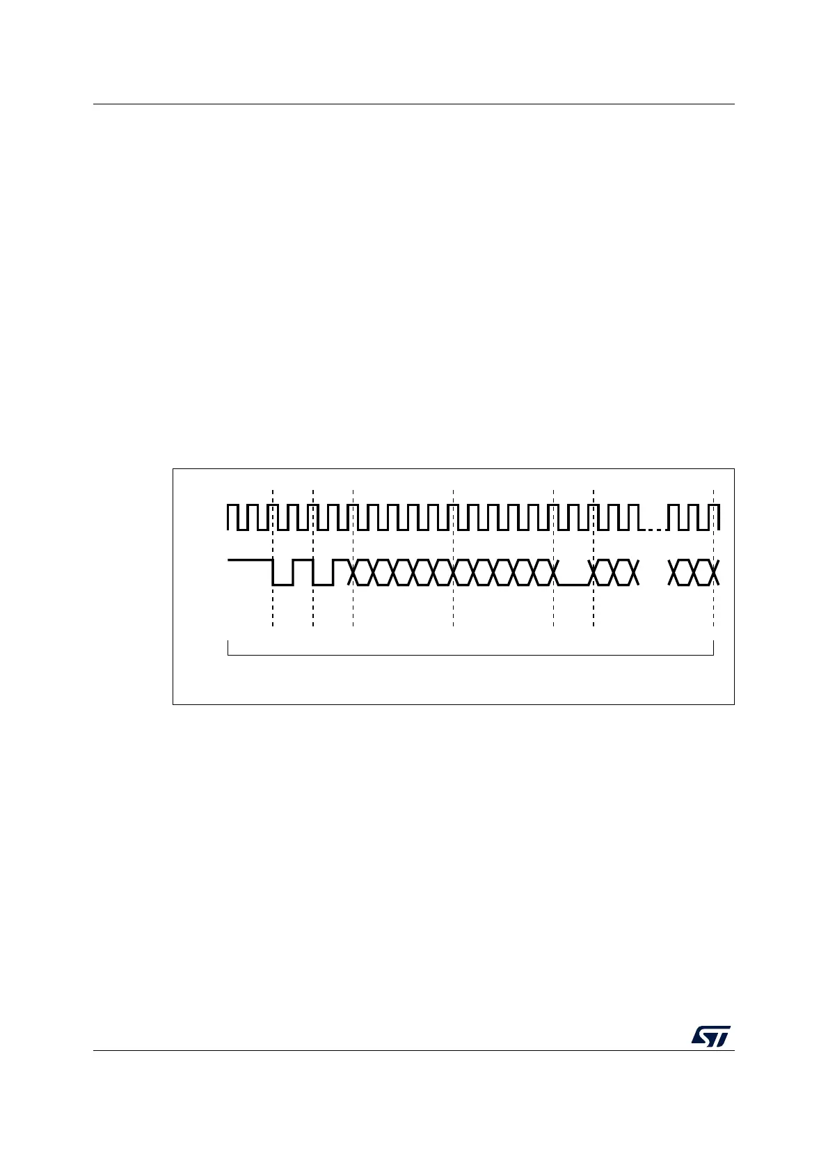
For a write transaction, the MAC controller drives a <10> pattern during the TA field.
The PHY device must drive a high-impedance state for the 2 bits of TA.
• Data: the data field is 16-bit. The first bit transmitted and received must be bit 15 of the
ETH_MIID register.
• Idle: the MDIO line is driven in high-impedance state. All three-state drivers must be
disabled and the PHY’s pull-up resistor keeps the line at logic one.
SMI write operation
When the application sets the MII Write and Busy bits (in Ethernet MAC MII address register
(ETH_MACMIIAR)), the SMI initiates a write operation into the PHY registers by transferring
the PHY address, the register address in PHY, and the write data (in Ethernet MAC MII data
register (ETH_MACMIIDR). The application should not change the MII Address register
contents or the MII Data register while the transaction is ongoing. Write operations to the MII
Address register or the MII Data register during this period are ignored (the Busy bit is high),
and the transaction is completed without any error. After the Write operation has completed,
the SMI indicates this by resetting the Busy bit.
Figure 315 shows the frame format for the write operation.
Figure 315. MDIO timing and frame structure - Write cycle
SMI read operation
When the user sets the MII Busy bit in the Ethernet MAC MII address register
(ETH_MACMIIAR) with the MII Write bit at 0, the SMI initiates a read operation in the PHY
registers by transferring the PHY address and the register address in PHY. The application
should not change the MII Address register contents or the MII Data register while the
transaction is ongoing. Write operations to the MII Address register or MII Data register
during this period are ignored (the Busy bit is high) and the transaction is completed without
any error. After the read operation has completed, the SMI resets the Busy bit and then
updates the MII Data register with the data read from the PHY.
Figure 316 shows the frame format for the read operation.
MDC
MDIO
32 1's 0 1
0
1 A4 A3 A2 A1 A0 R4 R3 R2 R1 R0
D15 D14
D1 D0
Preamble
Start
of
frame
OP
code
PHY address Register address
Turn
around
data
Data to PHY
ai15626
 Loading...


