Power control (PWR) RM0033
80/1381 RM0033 Rev 9
d) Enable the RTC TimeStamp interrupt
e) Re-enter the low-power mode
4.4 Power control registers
The power control registers can be accessed by half-words (16 bits) or words (32 bits).
4.4.1 PWR power control register (PWR_CR)
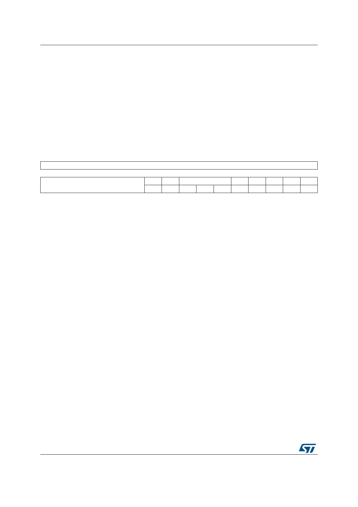
Address offset: 0x00
Reset value: 0x0000 0000 (reset by wakeup from Standby mode)
31 30 29 28 27 26 25 24 23 22 21 20 19 18 17 16
Reserved
1514131211109876543210
Reserved
FPDS DBP PLS[2:0] PVDE CSBF CWUF PDDS LPDS
rw rw rw rw rw rw rc_w1 rc_w1 rw rw
Bits 31:10 Reserved, always read as 0.
Bit 9 FPDS: Flash power down in Stop mode
When set, the Flash memory enters power down mode when the device enters Stop mode.
This allows to achieve a lower consumption in stop mode but a longer restart time.
0: Flash memory not in power down when the device is in Stop mode
1: Flash memory in power down when the device is in Stop mode
Bit 8 DBP: Disable backup domain write protection
In reset state, the RCC_BDCR register, the RTC registers (including the backup registers),
and the BRE bit of the PWR_CSR register, are protected against parasitic write access. This
bit must be set to enable write access to these registers.
0: Access to RTC and RTC Backup registers and backup SRAM disabled
1: Access to RTC and RTC Backup registers and backup SRAM enabled
Bits 7:5 PLS[2:0]: PVD level selection
These bits are written by software to select the voltage threshold detected by the Power
Voltage Detector
000: 2.0 V
001: 2.1 V
010: 2.3 V
011: 2.5 V
100: 2.6 V
101: 2.7 V
110: 2.8 V
111: 2.9 V
Note: Refer to the electrical characteristics of the datasheet for more details.
Bit 4 PVDE: Power voltage detector enable
This bit is set and cleared by software.
0: PVD disabled
1: PVD enabled
 Loading...


