3. SIGNALS AND WIRING
3 - 60
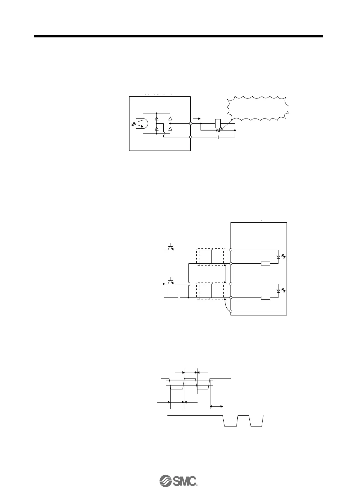
(2) Digital output interface DO-1
This is a circuit in which the emitter side of the output transistor is the output terminal. When the output
transistor is turned on, the current flows from the output terminal to a load.
A maximum of 2.6 V voltage drop occurs in the driver.
(Note) 24 V DC ± 10%
500 mA
Servo amplifier
ALM
etc.
DOCOM
Load
If polarity of diode is
reversed, servo amplifier
will malfunction.
If the voltage drop (maximum of 2.6 V) interferes with the relay operation, apply high
voltage (maximum of 26.4 V) from external source.
(3) Pulse train input interface DI-2
Give a pulse train signal in the open-collector type.
1) Interface
Max. input pulse
frequency 200 kpulses/s
Approx.
1.2 k Ω
Approx.
1.2 k Ω
Servo amplifier
PP2
PG
VCES ≤ 1.0 V
ICEO ≤ 100 μA
(Note)
Approx. 20 mA
Approx. 20 mA
(Note)
NP2
SD
NG
VCES ≤ 1.0 V
ICEO ≤ 100 μA
24 V DC ± 10%
500 mA
Pulse train input interface is comprised of a photocoupler.
If a resistor is connected to the pulse train signal line, it may malfunction due to
reduction in current.
0.9
0.1
tc tLH
tc tHL
tF
PP2
NP2
tLH = tHL < 0.2 µs
tc > 2 µs
tF > 3 µs
 Loading...