EasyManua.ls Logo

SMC Networks LECSB2-T Series

SMC Networks LECSB2-T Series
945 pages
To Next Page IconTo Next Page
To Previous Page IconTo Previous Page
Loading...
3. SIGNALS AND WIRING
3 - 59
(6) Analog output
Output voltage: ±10 V (Note 1, 2)
Maximum output current: 1 mA
Resolution: 10 bits or equivalent
LG
MO1
(MO2)
Servo amplifier
Note 1.
Output voltage range varies depending on the monitored signal.
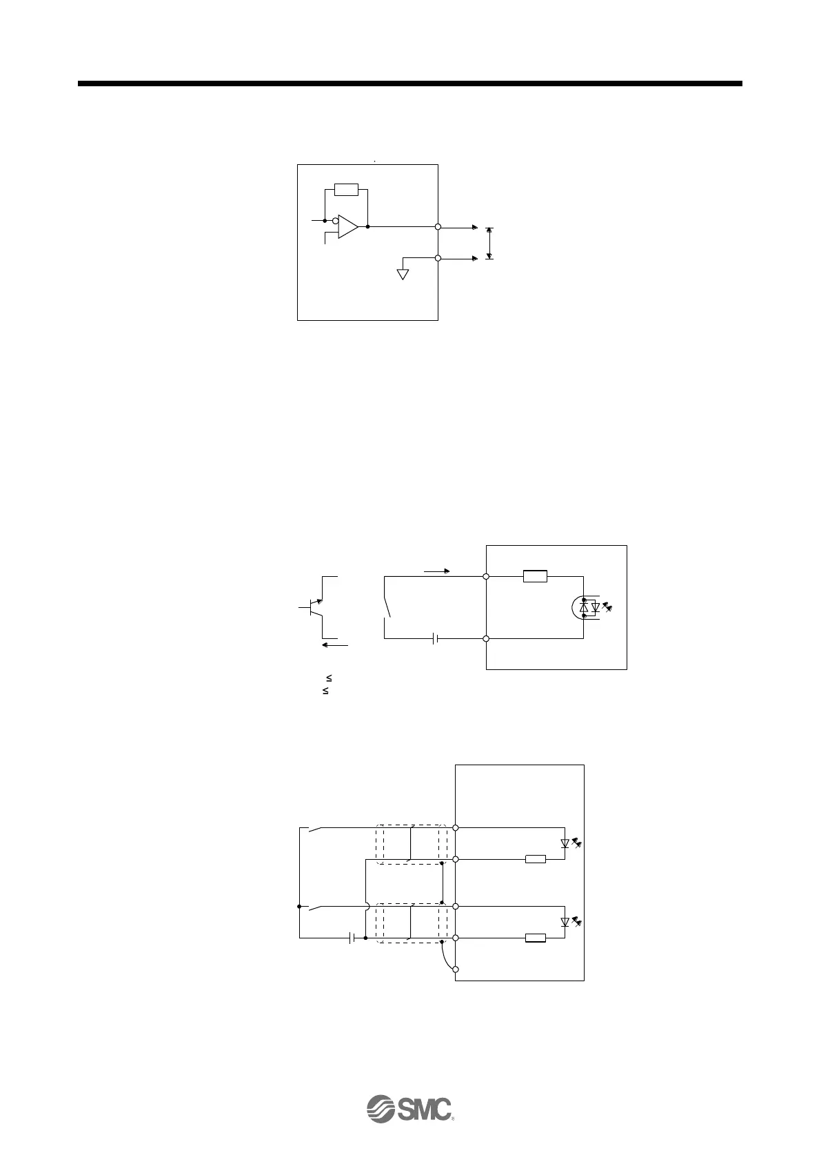
3.9.3 Source I/O interfaces
In this driver, source type I/O interfaces can be used.
(1) Digital input interface DI-1
This is an input circuit whose photocoupler anode side is the input terminal. Transmit signals using
source (open-collector) type transistor output, relay switch, etc. Additionally, the CN1-10 and CN1-35 pins
cannot be used for source inputs.
24 V DC ± 10%
500 mA
Switch
For transistor
EM2
etc.
Servo amplifier
DICOM
TR
Approximately
5 mA
V
CES
1.0 V
I
CEO
100 µA
Approximately
6.2 k Ω
The following shows when the CN1-37 pin and the CN1-38 pin are used as digital input interface:
Approximately
1.2 kΩ
Servo amplifier
PP2
(CN1-37)
PGSwitch
Approximately
1.2 kΩ
NP2
(CN1-38)
NG
SD
24 V DC ± 10%
500 mA
Switch
Driver
Driver
Driver

Table of Contents