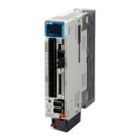
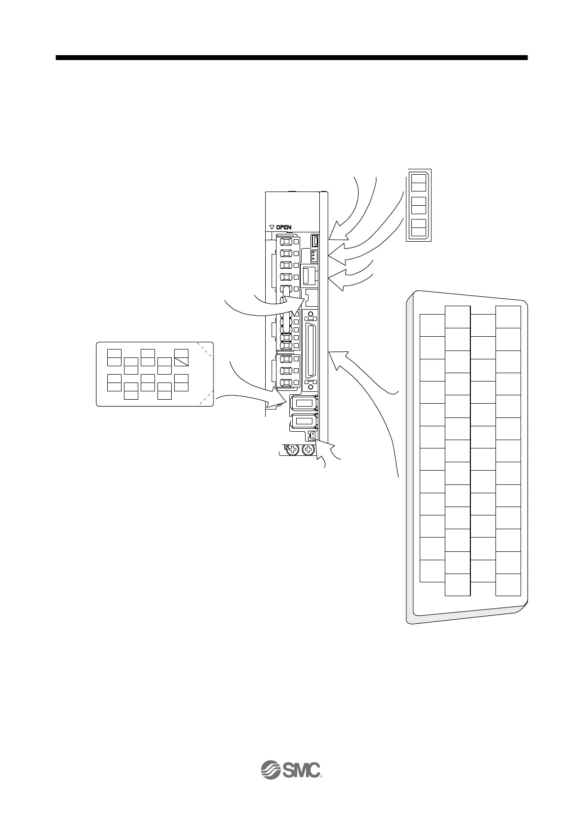
16.2.2 Connector and signal arrangement
The driver front view shown is that of the LECSB2-T7 or less. For other views of driver, connector
arrangements, and details, refer to chapter 9.
The device assignment of CN1 connector pins changes depending on the control mode. For the pins
which are given parameters in the related parameter column, their devices will be changed using those
parameters.
2
LG
3
MO2
1
MO1
CN6
CN1
The frame of the CN1 connector is connected
to the PE (grounding) terminal in the servo
amplifier.
CN5 (USB connector)
Refer to "MR-J4-_A_(-RJ) Servo
Amplifier Instruction Manual"
section 11.7.
CN3 (RS-422/RS485 connector)
Refer to "MR-J4-_A_(-RJ) Servo Amplifier
Instruction Manual" chapter 14.
This is a connector of 3M.
4
MRR
2
LG 8
6
1
P5
5
10
3
MR
7
9
BAT
(Note 2) CN2
MXR
MX
2
4
6
8
10
12
14
16
18
20
22
24
1
3
5
7
9
11
13
15
17
19
21
23
27
29
31
33
35
37
39
41
43
45
47
49
26
28
30
32
34
36
38
40
42
44
46
48
25 50
CN8
For the STO I/O signal connector,
refer to chapter 13.2 of
"MR-J4-_A_(-RJ) Servo Amplifier
Instruction Manual".
CN4 (battery connector)
Refer to "MR-J4-_A_(-RJ)
Servo Amplifier Instruction
Manual" section 11.8.
4
MRR2
2
LG 8
6
1
P5
5
10
3
MR2
7
9
(Note 1, 2) CN2L
(using serial encoder)
MXR2
THM2
THM1
MX2
BAT
4
PAR
2
LG 8
6
1
P5
PBR
PSEL
PB
5
10
3
PA
7
9
(Note 1, 2) CN2L
(using A/B/Z-phase pulse encoder)
PZR
PZ
 Loading...