Do you have a question about the AMD AMD5K86 and is the answer not in the manual?
Describes the notation used throughout the manual for clarity and consistency.
Defines key terms related to processor signals, bus cycles, and operations.
Lists the processor's standard features, high-performance aspects, and extensions.
Details the processor's cache and Translation Lookaside Buffer capabilities for enhanced performance.
Highlights processor extensions including CR4, new instructions, and MSRs.
Describes the processor's low-power design features and states.
Lists the processor's capabilities for testing and debugging system operation.
Explains the logic for fetching and decoding x86 instructions into internal ROPs.
Details the processor's pipeline stages and their impact on performance.
Describes the processor's instruction fetching mechanism and branch prediction.
Explains the two-stage decode logic and ROP generation process.
Details the processor's execution units and their operation.
Describes the two ALUs responsible for integer, logic, and shift operations.
Describes the IEEE 854-compatible floating-point unit and its execution capabilities.
Details the two load/store units for accessing data cache and memory operands.
Explains the branch unit's execution of predicted branches with zero delay.
Describes the reorder buffer (ROB) and store buffer for managing speculative execution.
Explains the retirement stage where results are written to real-state registers.
Discusses the on-chip instruction and data caches and their organization.
Details the characteristics of the 16-Kbyte instruction cache.
Describes the 8-Kbyte data cache and its MESI coherency protocol.
Explains the dual-tagged linear and physical cache tags.
Describes the process of filling cache lines from memory after a read miss.
Explains the cache-coherency mechanism based on MESI protocol.
Defines snooping actions like inquire cycles and internal snoops.
Describes various buffers associated with cache operations.
Details the speculative-state store buffer for managing outgoing operands.
Explains address translation using TLBs and page tables.
Details support for 4-Kbyte and 4-Mbyte paging with separate TLBs.
Describes bits in CR4 that enable architectural extensions like paging and VME.
Details support for 4-Mbyte pages and the associated 4-Mbyte TLB.
Explains how to make pages global for improved performance by retaining TLB entries.
Describes performance enhancements for 8086 programs in Virtual-8086 mode.
Describes support for interrupt virtualization in Protected mode.
Lists MSRs accessible via RDMSR/WRMSR instructions.
Describes the register for latching failed bus cycle addresses.
Describes the 64-bit counter incremented on each processor clock.
Lists instructions implemented by the AMD5K86 processor.
Describes the instruction for identifying processor type and features.
Covers general superscalar and AMD5K86-specific optimization techniques.
Discusses optimization techniques common to superscalar processors.
Details optimizations unique to the AMD5K86 processor.
Documents functional unit usage and cycle numbers for ROPs.
Defines mnemonics and operand types used in timing tables.
Shows execution-unit usage and timing for integer instructions.
Details execution-unit usage and timing for floating-point instructions.
Summarizes processor signals, functional groups, and compatibility.
Differentiates interrupts and exceptions, defining terms used.
Describes differences in bus signals between AMD5K86 and Pentium processors.
Provides detailed descriptions of each processor signal.
Explains the signal that clears bit 20 of the address bus in Real mode.
Explains the signal to obtain control of the address bus for inquire cycles.
Describes the signal to force the processor off the bus.
Explains the signal specifying a burst cycle.
Explains the signal indicating data or code access.
Describes signal that delays writes when external buffers are not empty.
Describes the signal causing writeback and invalidation of cache lines.
Explains the signal indicating an inquire cycle hit a modified line.
Explains the signal acknowledging a HOLD request.
Explains the signal to request control of the bus.
Explains the signal for reinitializing resources and invoking BIST.
Explains the signal that causes interrupt acknowledgment.
Explains the signal preserving integrity of bus cycle sequences.
Explains the signal causing entry into System Management Mode.
Explains the input signal to complete bus cycles and enter low-power states.
Explains the signal indicating a write or read cycle.
Explains signals specifying data-cache MESI state for read misses and write hits.
Summarizes bus cycle features like definition, addressing, alignment, and priorities.
Defines bus cycle types and signal usage.
Describes how addresses are driven on the bus.
Defines aligned and misaligned transfers for bus cycles.
Explains how bus access is managed by system logic.
Describes timing and signal relationships during various bus cycles.
Describes memory and I/O bus cycles transferring 1, 2, 4, or 8 bytes.
Describes cycles with four sequential eight-byte transfers.
Describes writebacks to memory of modified cache lines.
Explains how system logic obtains bus control and drives inquire cycles.
Illustrates an AHOLD-initiated inquire cycle that results in a cache miss.
Illustrates an AHOLD-initiated inquire cycle hitting a modified cache line.
Describes the BOFF signal for forcing the processor off the bus.
Explains the processor assertion of LOCK for bus cycle integrity.
Illustrates a Translation Lookaside Buffer miss for a 4-Kbyte page.
Describes the bus behavior for acknowledging an INTR interrupt.
Explains how various signals define special bus cycles.
Summarizes topics on system-management, clocking, and initialization.
Shows the processor's transition to System Management Mode (SMM).
Discusses processor configuration for memory bus speeds and DRAM types.
Shows a typical physical memory map for DOS-based systems.
Discusses system-defined cacheable address spaces.
Explains the cacheability of System Management Mode memory space.
Summarizes principles for controlling bus access and memory coherency.
Discusses implementation of L2 cache for performance improvement.
Explains how signals like PCD, CACHE, KEN, PWT control caching.
Compares writethrough and writeback cache protocols.
Explains how system logic drives inquire cycles for cache coherency.
Describes signals used to obtain bus control for inquire cycles.
Explains AHOLD's function for supporting inquire cycles.
Describes the protocol combining writethrough and writeback features.
Describes SMM as an interrupt-performed mode for power management.
Lists SMM environment features and initial register states.
Details the SMM state-save area map and its contents.
Discusses controlling processor power by reducing clock frequencies.
Lists the five states in the processor's clock-control protocol.
Describes the processor entering the Halt state via the HLT instruction.
Explains entering the Stop Grant state upon STPCLK assertion.
Describes the minimum power state where CLK is turned off.
Provides design rules to minimize circuit noise.
Details the HWCR format and fields for configuration bits.
Lists types of built-in self-tests: normal and TAP BIST.
Explains array testing using the Array Access Register (AAR).
Describes the MSR for testing cache and TLB arrays.
Mentions standard debug functions and I/O breakpoint extension.
Describes special bus cycles for tracing branch information.
Describes real-time testing using two processors in a master-checker setup.
Explains the JTAG standard for testing complex logic circuits.
Describes the tool for debugging via signals, registers, and microcode.
Compares AMD5K86 features with Pentium and 486 processors.
Compares AMD5K86 and Pentium processor signals.
Details differences in bus interface behavior compared to Pentium.
Compares misaligned memory and I/O cycle order with Pentium.
Compares selectable drive strengths with Pentium processor.
Discusses AHOLD Snoop and BOFF Asserted behavior.
Compares DCACHE write hit behavior with Pentium processor.
Compares memory management features with Pentium and 486 processors.
Notes AMD5K86 does not perform speculative TLB refills.
Compares power saving features with Pentium processor.
Compares STPCLK behavior in Halt state with Pentium processor.
Compares processor response to simultaneous SMI and debug traps.
Compares NMI recognition during SMM with Pentium processor.
Compares exception handling behavior with Pentium and 486 processors.
Compares prioritization of limit violation vs. invalid opcode faults.
Compares busy bit setting behavior during task switches.
Highlights differences in debug functions compared to Pentium.
Compares serial vs. merged processing of debug conditions.
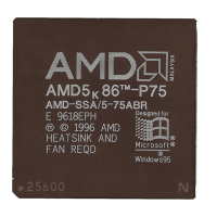
| Architecture | x86 |
|---|---|
| Core Count | 1 |
| Clock Speed | 133 MHz |
| FSB | 33 MHz |
| Voltage | 3.3V |
| L1 Cache | 16 KB |