3. SIGNALS AND WIRING
3 - 56
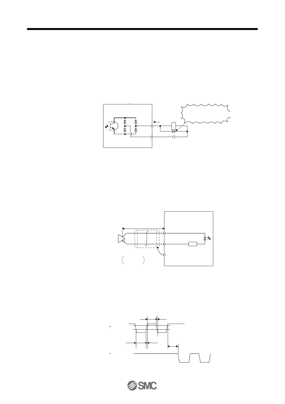
(2) Digital output interface DO-1
This is a circuit in which the collector of the output transistor is the output terminal. When the output
transistor is turned on, the current will flow to the collector terminal.
A lamp, relay or photocoupler can be driven. Install a diode (D) for an inductive load, or install an inrush
current suppressing resistor (R) for a lamp load.
(Rated current: 40 mA or less, maximum current: 50 mA or less, inrush current: 100 mA or less) A
maximum of 2.6 V voltage drop occurs in the driver.
The following shows a connection diagram for sink output. Refer to section 3.9.3 for source output.
(Note) 24 V DC ± 10%
500 mA
If polarity of diode is
reversed, servo amplifier
will malfunction.
Servo amplifier
ALM
etc.
Load
DOCOM
If the voltage drop (maximum of 2.6 V) interferes with the relay operation, apply high
voltage (maximum of 26.4 V) from external source.
(3) Pulse train input interface DI-2
Give a pulse train signal in the differential line driver type or open-collector type.
(a) Differential line driver type
1) Interface
SD
PG (NG)
PP (NP)
Max. input pulse
frequency 4 Mpulses/s
(Note 2)
Servo amplifier
Am26LS31 or equivalent
Approximately
100 Ω
V
OH
: 2.5 V
V
OL
: 0.5 VV
(Note 1)
10 m or less
Pulse train input interface is comprised of a photocoupler.
If a resistor is connected to the pulse train signal line, it may malfunction due to
reduction in current.
When the input pulse frequency is 4 Mpulses/s, set [Pr. PA13] to "_ 0 _ _".
0.9
0.1
tc tLH
tc tHL
tF
PP PG
NP NG
tLH = tHL < 50 ns
tc > 75 ns
tF > 3 µs
 Loading...