Circuit Pack Descriptions
7-72 Issue 8.0 July 2002
General Description of Operation 7
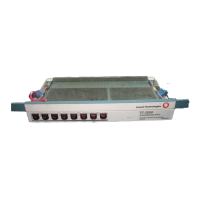
The OC12 circuit pack provides a bi-directional interface between an OC-12/12C
optical line (622.08 MHz) and electrical STS-3 rate (155.52 MB/s) backplane
interface signals. In the FT-2000 OC-48 lightwave system, the OC-12/12C circuit
packs are physically located in the OC-48 LS shelf. The circuit pack assembly is
four slots wide and has four connectors to pick up and drop STS3 rate signals
from each of the slots. The slot location for the OC12 circuit pack is identified by
the left most slot, and the only allowable locations for plugging in the OC12 pack
are slots 1A, 3A, 5A, and 7A. While the left most slot is used for identifying the
circuit pack’s location in the backplane connector for powering and the board
controller interfaces; i.e., the main connector slots corresponding to the circuit
pack locations 1A, 3A, 5A, and 7A are slots 1B, 3B, 5B, and 7B respectively.
In the transmit direction, (OC-12/12C line in to the LS backplane out), the OC12
circuit pack converts the OC-12/12C optical input signal into an electrical
STS-12/12C signal which is demultiplexed into four STS-3 rate signals. The four
STS-3 rate signals are synchronized to the system clock and distributed to the
backplane as data-only signals.
In the receive direction (LS backplane in to OC-12/12C line out), the OC12 circuit
pack selects four of the electrical STS-3 rate signals from the service or protection
OC-48 receivers in the HS shelf. These four signals are then synchronized to the
system clock and multiplexed into an STS-12/12C signal which drives a laser
transmitter.
The control and monitoring of the OC12 circuit pack is done by the board
controller through GPID leads and the SDSI (SONET device serial interface)
leads.