Circuit Pack Descriptions
Issue 8.0 July 2002
7-89
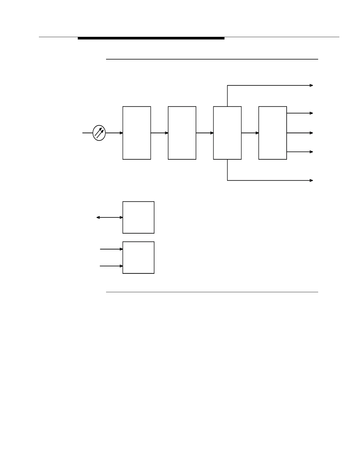
Figure 7-27. OC48 RCVR A/D (839B2 and 839B4B) Circuit Pack Block
Diagram
The optical-to-electrical converter receives the OC-48 signal and converts it to an
electrical STS-48 signal. The optical-to-electrical converter also detects OC-48
loss of signal (LOS). Timing is also extracted and the data is regenerated. The
STS-48 data signal and 2.5 GHz clock signal are then passed to the byte
demultiplexer.
The byte demultiplexer receives the STS-48 data signal from the
optical-to-electrical converter and demultiplexes the STS-48 data signal into
sixteen 155.52 Mb/s data signals. The sixteen 155.52 Mb/s data signals and a
155.52 MHz clock signal are sent to the receive byte processor.
155 Mb/s
Signals
SONET Overhead
BCLAN
OC-48
25.92 MHz Timing
Switch
Matrix
Receive
Byte
Processor
Byte
Demux
Optical
To
Electrical
Module
Board
Controller
Circuit
Power
Circuit
-48 V (A)
-48 V (B)