Circuit Pack Descriptions
7-100 Issue 8.0 July 2002
Detailed Description of Operation 7
Transmission Circuitry 7
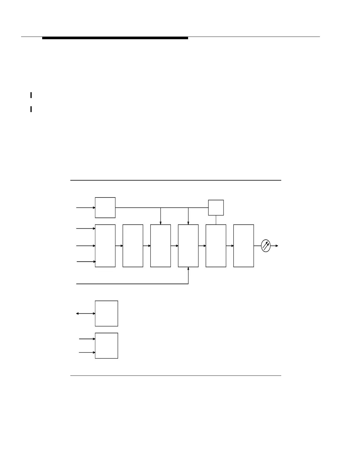
Figure 7-30 shows an overall block diagram of the 739B2, 739B4, 739C2, 739J2,
739J3, 739J4, 739R2, and 739S2 OC48 TRMTR A/D circuit packs. Figure 7-31
shows an overall block diagram of the 739E[1-16], 739G[1-8], 739H[1-16], 739J5,
739P5, 739R5, and 739S5 OC48 TRMTR A/D circuit packs. The OC48 TRMTR
A/D circuit packs interface with up to three different buses (add/drop, high speed
protection, and through) that carry up to eighteen 155.52 Mb/s signals each
(sixteen service and two protection). The add/drop bus provides access to the
155.52 Mb/s signals from the low speed interface circuit packs. The high speed
protection bus provides access to the 155.52 Mb/s signals from the OC48 RCVR
A/D circuit pack in the same direction for high speed line protection switching. The
through bus provides access to the 155.52 Mb/s signals from the OC48 RCVR
A/D circuit pack that are passed through in bidirectional ring applications.
Figure 7-30. OC48 TRMTR A/D (739B2, 739B4, 739C2, 739J2, 739J3,
739J4, 739R2, and 739S2) Circuit Pack Block Diagram
155 Mb/s
PLL
Signals
SONET Overhead
BCLAN
OC-48
-48V(A)
-48V(B)
155.52 MHz
Timing
Electrical
To
Optical
Module
Byte
Multiplexer
Transmit
Byte
Processor
Pointer
Processor
Timing
Recovery
Switching
Matrix
Timing
Interface
Board
Controller
Circuit
Power
Circuit