Circuit Pack Descriptions
Issue 8.0 July 2002
7-119
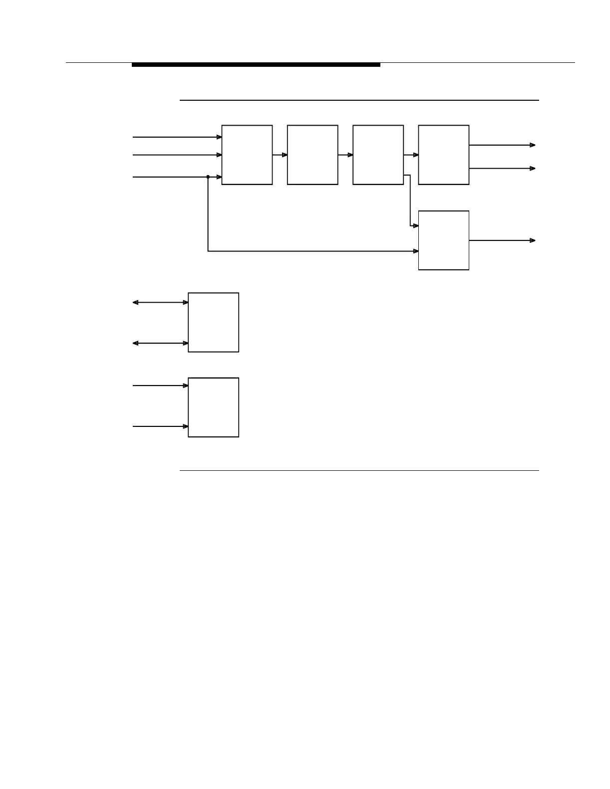
Figure 7-35. TG3 (DS1) (LAA18) Circuit Pack Block Diagram
Timing Circuitry 7
Reference Input Interface Circuit. 7The reference input interface circuit provides
the required interface to all the reference inputs and selects one of the inputs as
the timing reference. The reference input interface circuit interfaces with the
following references:
■ One external DS1 reference signal (1.544 MHz) from a stratum 3 or better
source
■ One line reference signal (25.92 MHz) from the OC48 Receiver circuit pack
(up to four line reference signals in a future release)
■ One cross-coupled reference signal (25.92 MHz) from the companion TG3
(DS1) circuit pack.
-48V (A)
TG3
Power
Board
Controller
Circuit
Companion
BCLAN
DS1 Reference
Cross-Coupled Reference
Reference
Input
Jitter
Reduction
Interface
-48V (B)
Circuit
Output
Drivers
Timing For
Reference
Cross-Coupled
Digital
PLL
Transmit Circuits
DS1
Reference
Interface
DS1 Reference
Line Reference