Zynq-7000 AP SoC and 7 Series FPGAs MIS v4.1 103
UG586 November 30, 2016
www.xilinx.com
Chapter 1: DDR3 and DDR2 SDRAM Memory Interface Solution
AXI4-Lite Slave Control/Status Register Interface Signals
Table 1-22 lists the AXI4 slave interface specific signals. Clock/reset to the interface is
provided from the Memory Controller.
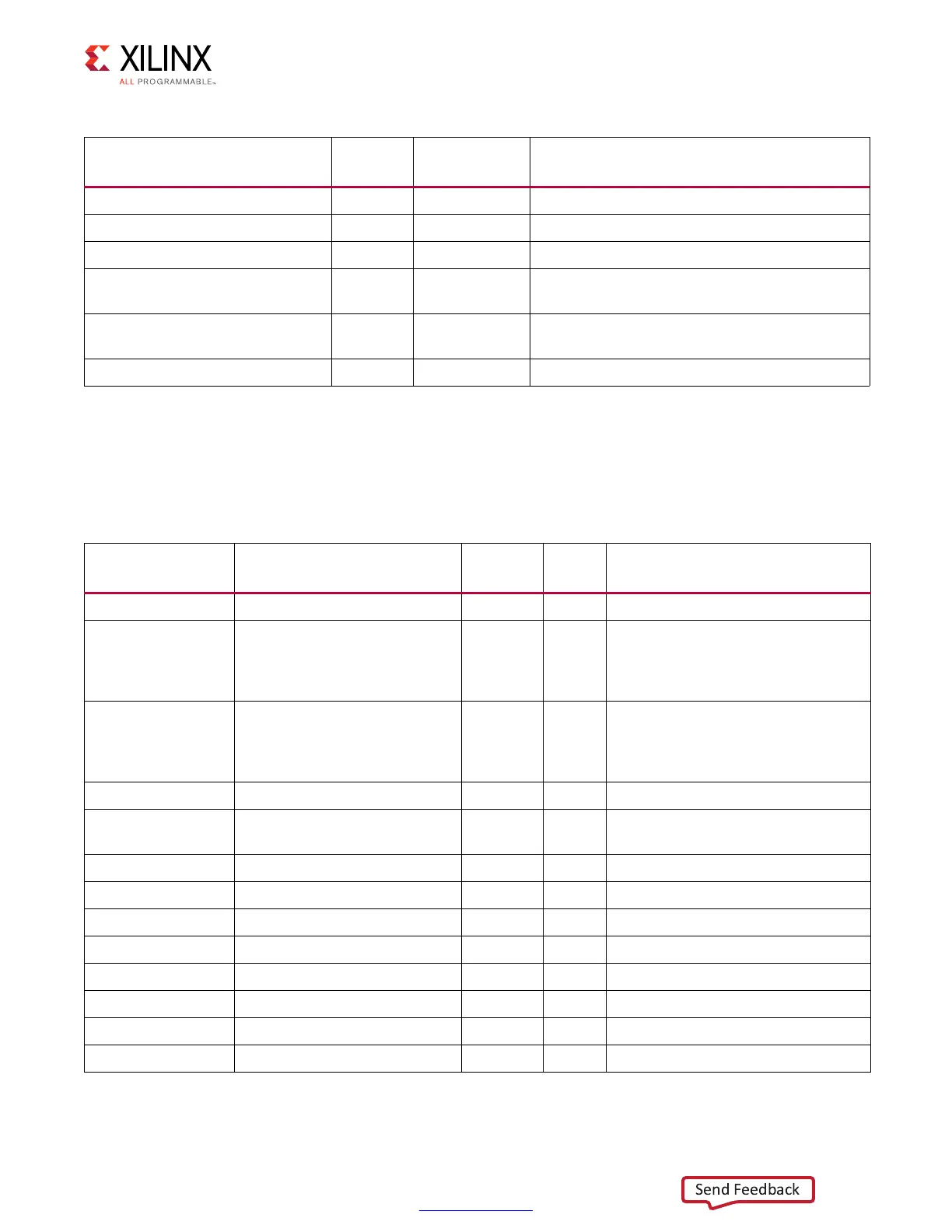
Table 1-21: AXI4-Lite Slave Control/Status Register Parameters
Parameter Name
Default
Value
Allowable
Values
Description
C_S_AXI_CTRL_ADDR_WIDTH 32 32, 64 This is the width of the AXI4-Lite address buses.
C_S_AXI_CTRL_DATA_WIDTH 32 32 This is the width of the AXI4-Lite data buses.
C_ECC_ONOFF_RESET_VALUE 1 0, 1 Controls ECC on/off value at startup/reset.
C_S_AXI_CTRL_BASEADDR – Valid Address
This parameter specifies the base address for
the AXI4-Lite slave interface.
C_S_AXI_CTRL_HIGHADDR – Valid Address
This parameter specifies the high address for
the AXI4-Lite slave interface.
C_S_AXI_CTRL_PROTOCOL AXI4LITE AXI4LITE AXI4-Lite protocol
Table 1-22: List of New I/O Signals
Name Width Direction
Active
State
Description
s_axi_ctrl_awaddr C_S_AXI_CTRL_ADDR_WIDTH Input Write address.
s_axi_ctrl_awvalid 1 Input High
Write address valid. This signal
indicates that valid write address
and control information are
available.
s_axi_ctrl_awready 1 Output High
Write address ready. This signal
indicates that the slave is ready to
accept an address and associated
control signals.
s_axi_ctrl_wdata C_S_AXI_CTRL_DATA_WIDTH Input Write data
s_axi_ctrl_wvalid 1 Input High
Write valid. This signal indicates that
write data and strobe are available.
s_axi_ctrl_wready 1 Output High Write ready.
s_axi_ctrl_bvalid 1 Output High Write response valid.
s_axi_ctrl_bready 1 Input High Response ready.
s_axi_ctrl_araddr C_S_AXI_CTRL_ADDR_WIDTH Input Read address.
s_axi_ctrl_arvalid 1 Input High Read address valid.
s_axi_ctrl_arready 1 Output High Read address.
s_axi_ctrl_rdata C_S_AXI_CTRL_DATA_WIDTH Output Read data.
s_axi_ctrl_rvalid 1 Output Read valid.
 Loading...


