Zynq-7000 AP SoC and 7 Series FPGAs MIS v4.1 329
UG586 November 30, 2016
www.xilinx.com
Chapter 2: QDR II+ Memory Interface Solution
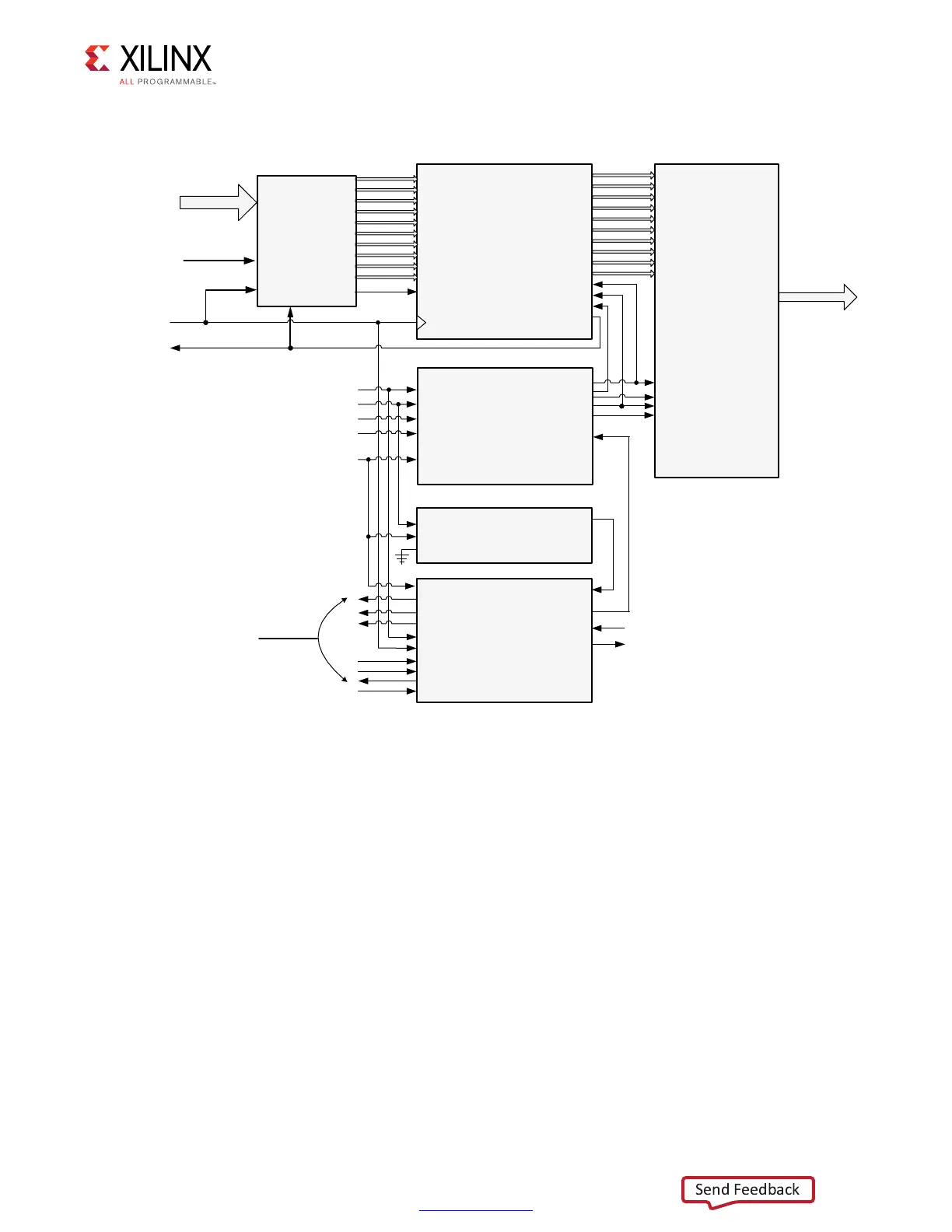
The clocking details of the address/control using PHASER_OUT are shown in Figure 2-45.
Output Path
Because the address/command and write data are provided by the user backend, the QDR
PHY transfers the signals from the FPGA logic domain to their internal PHASER clock
domain and provides them from the OSERDES to the memory. The OUT_FIFOs are used
mainly as domain transfer elements in the design, and therefore the write and read enables
of the OUT_FIFO need to be constantly enabled. The PHY Control block helps with this
requirement.
X-Ref Target - Figure 2-45
Figure 2-45: Address Path
/54?&)&/
$;=
234
72#,+
2$#,+
2$%.
&5,,
$;=
$;=
$;=
$;=
$;=
$;=
$;=
$;=
$;=
&2%
1""
72%.
1;=
1;=
1;=
1;=
1;=
1;=
1;=
1;=
1;=
1;=
-%-2%&#,+
&2%12%&#,+
&).%%.!",%
&).%).#
/#,+$)6
/#,+
/#,+$%,!9%$
/3%2$%3234
/,/')#
/3%2$%3
/$$2
0HY
?WR?EN
/F?FULL
&ROM0,,
&ROM0,,
0(!3%2 ?/54 ?0(9
0(!3%2 ?2%&
0(9 ?#/.42/,
#,+).
,/#+%$
072$7.
234
0(9#4,!,-/34&5,,
0(9#4,&5,,
0(9#4,%-049
0(9#4,2%!$9
-%-2%&#,+
0(9#,+
0(9#4,-342%-049
0(9#4,7$
0(9#4,72%.!",%
0,,,/#+
2%&$,,,/#+
2%3%4
39.#).
/54"52340%.$).'
&ROM0,,
4O &ROM
)NITIALIZATION
,OGIC
RST
"52340%.$).'0(9
234
&ROM-ASTER
PHY?CONTROL
4OOTHER
PHY?CONTROL
BLOCKS
OUTPUTDATATOA
BYTEGROUP
7RITE?ENABLE
FROMFABRIC
02%?&)&/
$
1
#,+
72%.
0HY?CLK
2$%.!",%
&ABRIC0(!3%2?/54DLY
CONTROLSTOPROVIDE
DEGREEPHASESHIFTTO
ADDRESSCONTROLSIGNALS
1
/3%2$%3/0TO
12))MEMORY
QDR?SAQDR?R?N
QDR?W?N
5'?C??
 Loading...


