Zynq-7000 AP SoC and 7 Series FPGAs MIS v4.1 392
UG586 November 30, 2016
www.xilinx.com
Chapter 3: RLDRAM II and RLDRAM 3 Memory Interface Solutions
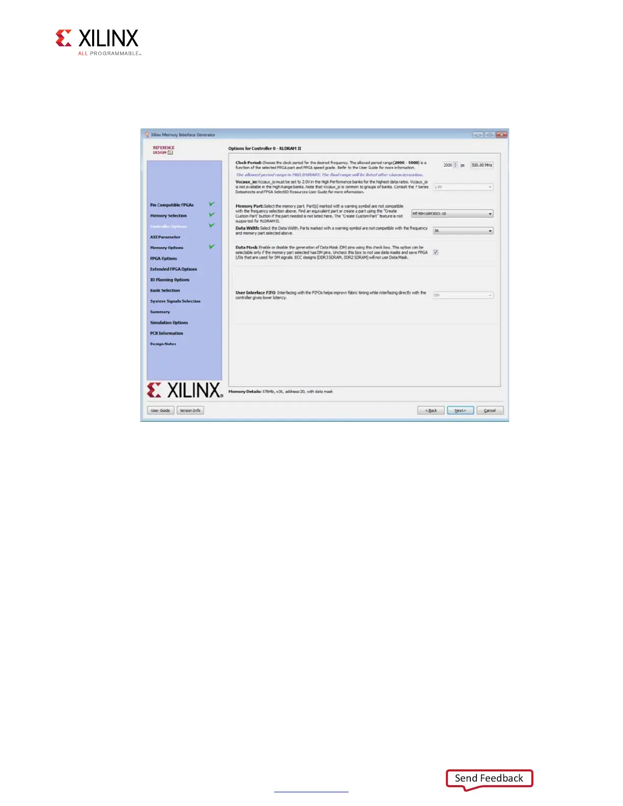
Controller Options
This page shows the various controller options that can be selected.
• Frequency – This feature indicates the operating frequency for all the controllers. The
frequency block is limited by factors such as the selected FPGA and device speed grade.
• PHY to Controller Clock Ratio – This feature determines the ratio of the physical layer
(memory) clock frequency to the controller and user interface clock frequency. The user
interface data bus width of the 2:1 ratio is four times the width of the physical memory
interface width, while the bus width of the 4:1 ratio is eight times the physical memory
interface width. RLDRAM II must use 2:1 while RLDRAM 3 must use 4:1.
• VCCAUX_IO – Set based on the period/frequency setting. 2.0V is required at the
highest frequency settings in the High Performance column. The MIG tool
automatically selects 2.0V when required. Either 1.8 or 2.0V can be used at lower
frequencies. Groups of banks share the VCCAUX_IO supply. For more information, see
the 7 Series FPGAs SelectIO™ Resources User Guide (UG471) [Ref 2].
• Memory Part – This option selects the memory part for the design. Selections can be
made from the list, or if the part is not listed, a new part can be created (Create
Custom Part). If a desired part is not available in the list, you can generate or create an
equivalent device and then modify the output to support the desired memory device.
X-Ref Target - Figure 3-17
Figure 3-17: Controller Options Page
 Loading...


