Zynq-7000 AP SoC and 7 Series FPGAs MIS v4.1 608
UG586 November 30, 2016
www.xilinx.com
Chapter 4: LPDDR2 SDRAM Memory Interface Solution
Note that the expected data is generated using the same 64-bit LFSR logic that was used to
write the 128 long PRBS sequence to the SDRAM. The data mismatch tap value is recorded
as the left edge.
The algorithm then increments to the initial tap value and edge detection begins with every
increment after the initial tap value until a data mismatch is found or the tap value is 31. The
algorithm then computes the center of the read data valid window based on the detected
edges.
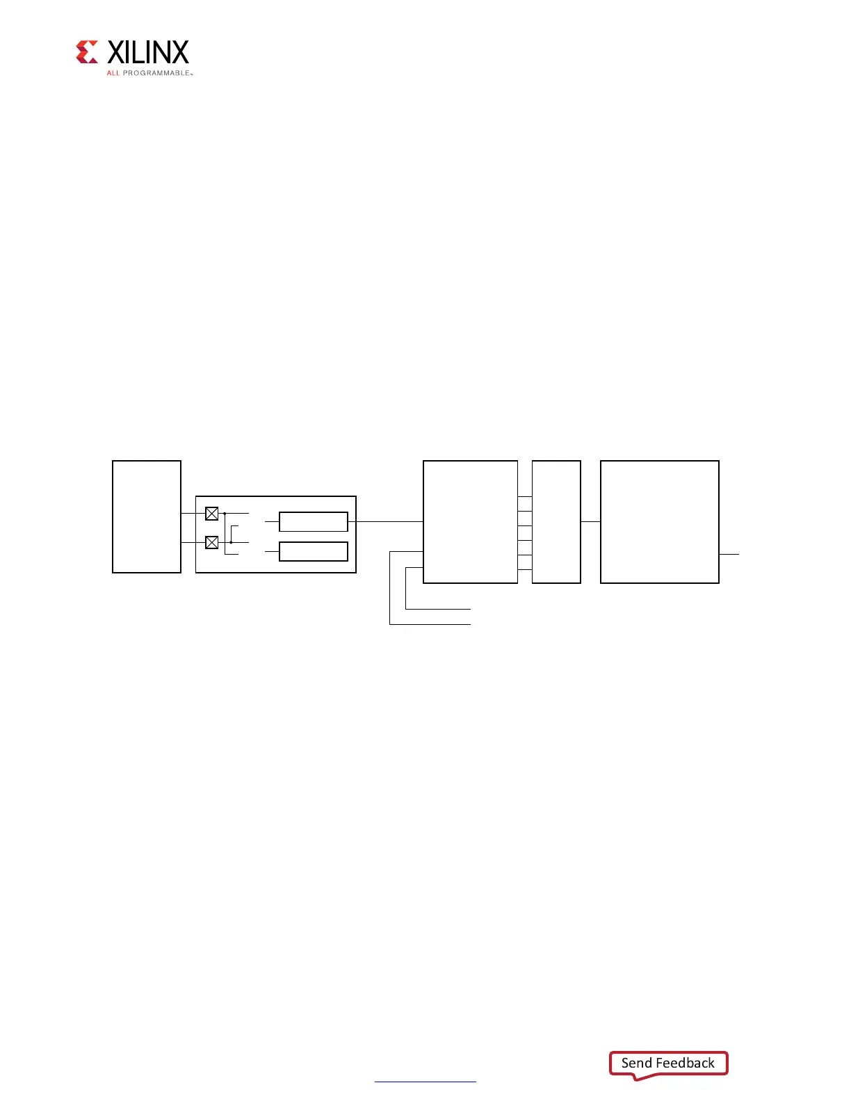
Phase Detector
In the 7 series FPGA memory interface design, read DQ is not sampled by the
corresponding DQS signal. Instead, read DQ is sampled by a free-running clock operating at
the same frequency as the differential SDRAM CK/CK# signals. The free-running clock has a
single source for all DQ bits, but the phase of each byte capture clock output can be
separately adjusted using IODELAY elements. The phase detector initially locks the phase of
each byte-capture clock such that it is in phase with the corresponding DQS signal
(Figure 4-54).
Subsequent changes in capture timing delays after initial calibration due to voltage and
temperature changes can be compensated for by maintaining the phase relationship
between the byte-capture clock and the corresponding DQS. Periodic dummy reads are
required from the Memory Controller to dynamically maintain phase lock between the
byte-capture clock and DQS (Figure 4-55).
Periodic compensation can be accomplished by adjusting the phase of the
MMCM-generated source capture clock using the fine-phase shift capability of the MMCM.
This method allows fine adjustment of the capture clocks of all bytes simultaneously but
does not allow control over individual byte clock phase adjustment.
X-Ref Target - Figure 4-54
Figure 4-54: Phase Detector Block Diagram
,0$$2
3$2!-
)/$%,!9
$13
1
RD?DQS?DATA;=
CLK?RSYNC
"YTE#APTURE#LOCK
PD?CAL?DONE
5'?C??
1
1
1
1
1
$13
)3%2$%3
$13
0HASE
$ETECTOR
2EAD
"ITSLIP
)/$%,!9
 Loading...


