Zynq-7000 AP SoC and 7 Series FPGAs MIS v4.1 170
UG586 November 30, 2016
www.xilinx.com
Chapter 1: DDR3 and DDR2 SDRAM Memory Interface Solution
Read Path
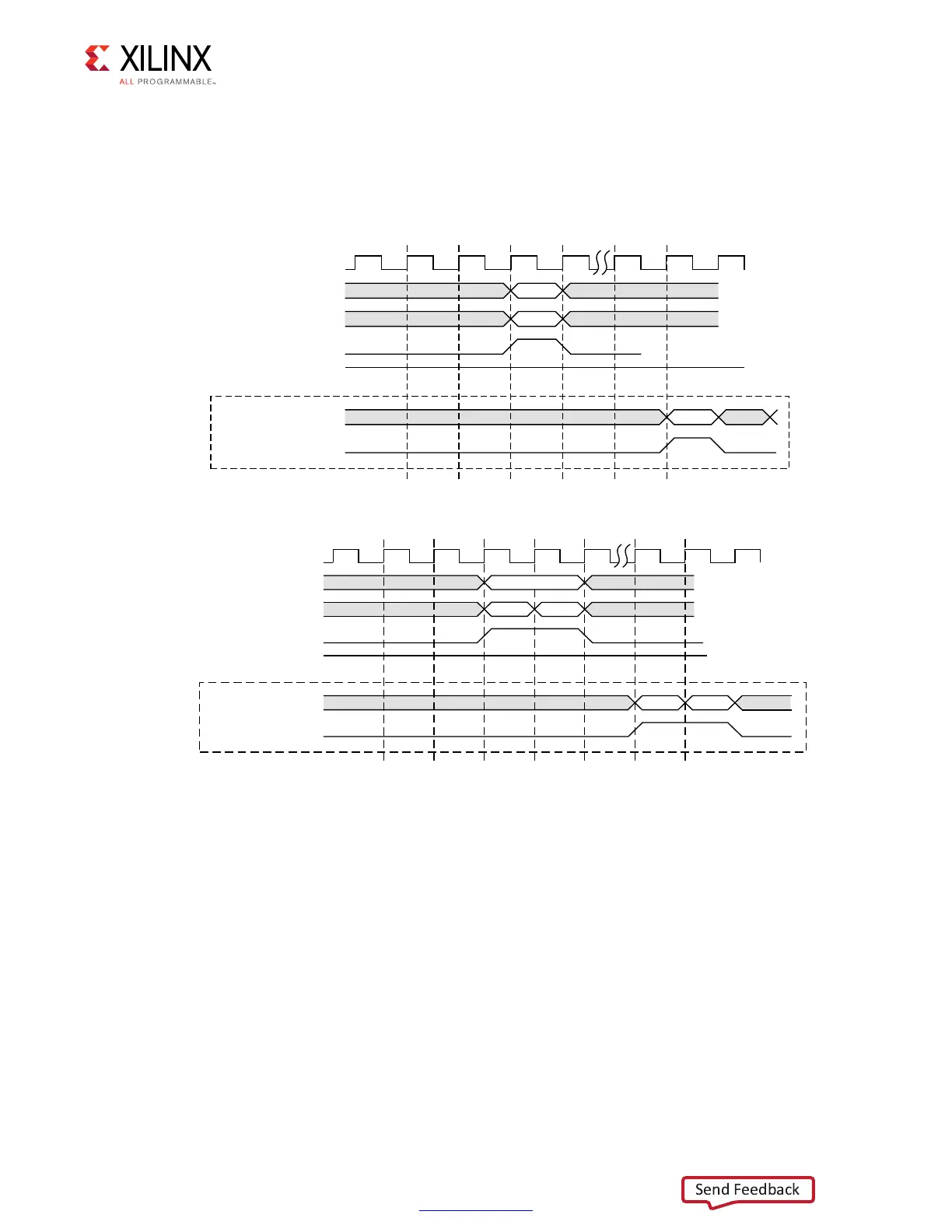
The read data is returned by the UI in the requested order and is valid when
app_rd_data_valid is asserted (Figure 1-81 and Figure 1-82). The app_rd_data_end
signal indicates the end of each read command burst and is not needed in user logic.
In Figure 1-82, the read data returned is always in the same order as the requests made on
the address/control bus.
User Refresh
For user-controlled refresh, the Memory Controller managed maintenance should be
disabled by setting the USER_REFRESH parameter to “ON.”
To request a REF command, app_ref_3req is strobed for one cycle. When the Memory
Controller sends the command to the PHY, it strobes app_ref_ack for one cycle, after
which another request can be sent. Figure 1-83 illustrates the interface.
X-Ref Target - Figure 1-81
Figure 1-81: 4:1 Mode UI Interface Read Timing Diagram (Memory Burst Type = BL8)
X-Ref Target - Figure 1-82
Figure 1-82: 2:1 Mode UI Interface Read Timing Diagram (Memory Burst Type = BL4 or BL8)
8*BFBB
DSSBUGBGDWD
FON
DSSBFPG
5
5($'
DSSBDGGU
$GGU
DSSBHQ
DSSBUGBGDWDBYDOLG
DSSBUG\
8*BFBB
DSSBUGBGDWD
FON
DSSBFPG
5
DSSBDGGU
$GGU
DSSBHQ
DSSBUGBGDWDBYDOLG
DSSBUG\
$GGU
5
5($'
 Loading...


