Zynq-7000 AP SoC and 7 Series FPGAs MIS v4.1 434
UG586 November 30, 2016
www.xilinx.com
Chapter 3: RLDRAM II and RLDRAM 3 Memory Interface Solutions
Clocking Architecture
The PHY design requires that an MMCM and a PLL module be used to generate various
clocks. Both global and local clock networks are used to distribute the clock throughout the
design.
The clock generation and distribution circuitry and networks drive blocks within the PHY
that can be divided roughly into four separate general functions:
• Internal FPGA logic
• Write path (output) logic
• Read path (input) and delay logic
• IDELAY reference clock (200 MHz)
One MMCM and one PLL is required for the PHY. The MMCM and PLL generate the clocks
for most of the internal logic, the input clocks to the phasers, and a synchronization pulse
required to keep the PHASER blocks synchronized in a multi-I/O bank implementation.
The PHASER blocks require three clocks:
• Memory Reference Clock – The memory reference clock is required to be at the same
frequency as that of the RLDRAM II/RLDRAM 3 memory interface clock.
• Frequency Reference Clock – The frequency reference clock must be equal to the
memory clock frequency for frequencies ≥ 400 MHz and 2x the memory clock
frequency for frequencies < 400 MHz such that it meets the reference range
requirement of 400 MHz to 1,066 MHz.
• Phase Reference Clock from the PLL – The phase reference clock is used in the read
banks, and is generated using the memory read clock (QK/QK#) routed internally and
provided to the Phaser logic to assist with data capture.
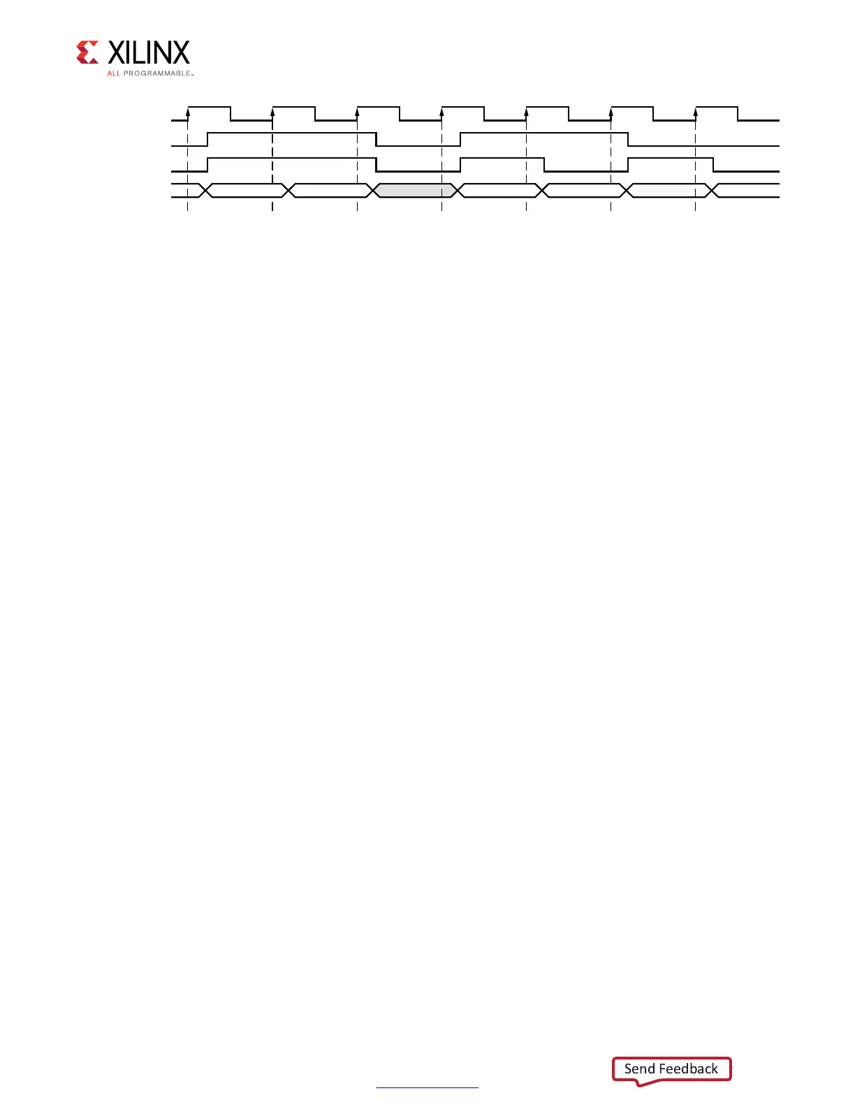
X-Ref Target - Figure 3-44
Figure 3-44: Client Interface Protocol Read Data
USER?RD?VALID;=
USER?RD?DATA
#,+
5'?C??
USER?RD?VALID;=
[FALLRISEFALLRISE] [FALLRISEFALLRISE] [FALLRISEFALLRISE] [$.#$.#FALLRISE] [FALLRISE$.#$.#]
 Loading...


