Zynq-7000 AP SoC and 7 Series FPGAs MIS v4.1 476
UG586 November 30, 2016
www.xilinx.com
Chapter 3: RLDRAM II and RLDRAM 3 Memory Interface Solutions
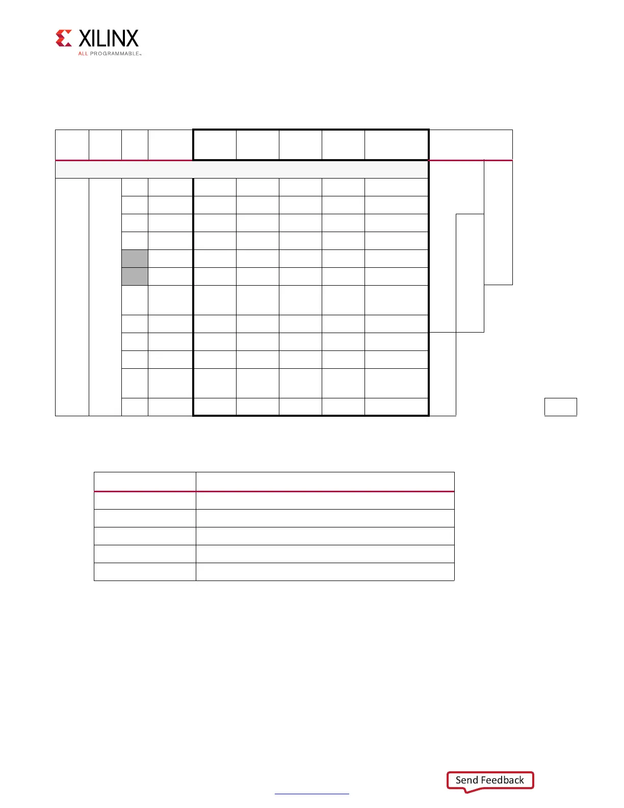
Table 3-22 shows the RLDRAM II byte lane with the 3-state pin location used for DM. In this
situation the signals are shifted down in the OUT_FIFO.
The byte lane parameters for Table 3-22 are shown in Table 3-23.
I/O Standards
The MIG tool generates the appropriate XDC for the core with SelectIO™ standards based
on the type of input or output to the 7 series FPGAs. These standards should not be
changed. Table 3-24 and Table 3-25 contain a list of the ports with the I/O standard used.
Table 3-22: Example RLDRAM II Byte Lane #5, Shared 3-State with DM in Byte Lane #2
Bank
Byte
Lane
Bit MAP DDR
Byte
Group
I/O
Type
I/O
Number
Special
Designation
BITLANES
XDC
02
9 DQ26 DQ26 C_11 P 12 1
8 DQ25 DQ25 C_10 N 11 1
7 DQ24 DQ24 C_09 P 10 1
6 DQ23 DQ23 C_08 N 9 1
B DQ22 DQ22 C_07 P 8 DQS-P 1 1111
A DM DM C_06 N 7 DQS-N 1 F
5 3-state DQ21 C_05 P 6 0
110
1
4 DQ21 DQ20 C_04 N 5 1 D
3 DQ20 DQ19 C_03 P 4 CCIO-P 1
2 DQ19 DQ18 C_02 N 3 CCIO-N 1
1DQ18QK1_P C_01 P 2 CCIO-P 1
111
0
0 QK1_N C_00 N 1 CCIO-N 0 EFDE
Table 3-23: Parameters for Example RLDRAM II Data Byte Lane #5
Parameter Value
DM_MAP 12'h02A
DQTS_MAP 12'h025
PHY_0_BITLANES 12'hFDE
DATA1_MAP 108'h029_028_027_026_02B_024_023_022_021
QK_MAP 8'h02
 Loading...


