Zynq-7000 AP SoC and 7 Series FPGAs MIS v4.1 475
UG586 November 30, 2016
www.xilinx.com
Chapter 3: RLDRAM II and RLDRAM 3 Memory Interface Solutions
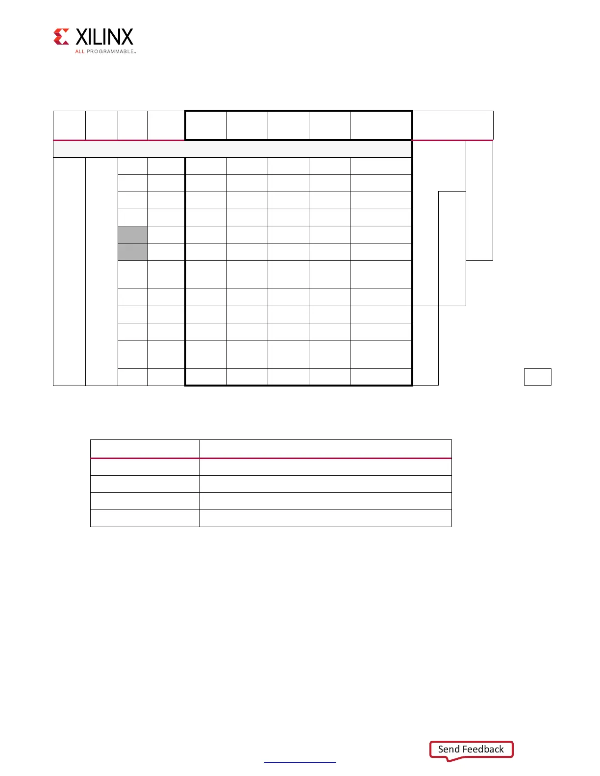
Table 3-20 shows another RLDRAM II byte lane with the 3-state control location unused.
The byte lane parameters for Table 3-20 are shown in Table 3-21.
Table 3-20: Example RLDRAM II Byte Lane #4, 3-State with Control Location Unused
Bank
Byte
Lane
Bit MAP DDR
Byte
Group
I/O
Type
I/O
Number
Special
Designation
BITLANES
XDC
02
9 DQ26 DQ26 C_11 P 12 1
8 DQ25 DQ25 C_10 N 11 1
7 DQ24 DQ24 C_09 P 10 1
6 DQ23 DQ23 C_08 N 9 1
B DQ22 DQ22 C_07 P 8 DQS-P 1 1011
AC_06N 7DQS-N0B
5 DQ21 DQ21 C_05 P 6 1
111
1
4 DQ20 DQ20 C_04 N 5 1 F
3 DQ19 DQ19 C_03 P 4 CCIO-P 1
2 DQ18 DQ18 C_02 N 3 CCIO-N 1
1 QK1_P C_01 P 2 CCIO-P 0
110
0
0 QK1_N C_00 N 1 CCIO-N 0 CBFC
Table 3-21: Parameters for Example RLDRAM II Data Byte Lane #4
Parameter Value
DQTS_MAP 12'h02A
PHY_0_BITLANES 12'hBFC
DATA1_MAP 108'h029_028_027_026_02B_025_024_023_022
QK_MAP 8'h02
 Loading...


