Zynq-7000 AP SoC and 7 Series FPGAs MIS v4.1 353
UG586 November 30, 2016
www.xilinx.com
Chapter 2: QDR II+ Memory Interface Solution
Debug Signals
The MIG tool includes a Debug Signals Control option on the FPGA Options screen.
Enabling this feature allows calibration, tap delay, and read data signals to be monitored
using the Vivado logic analyzer feature. Selecting this option port maps the debug signals
to VIO modules of the Vivado logic analyzer feature in the design top module.
Sample debug logic by connecting the debug ports to the Vivado Design Suite debug
feature modules (that is, ILA and VIO) is provided in the example design top
(example_top) module with a Debug Signals for Memory Controller option value of “ON.”
In User Design top, all debug port signals are grouped under a few buses and provided in
the port list.
To confirm that all debug ports are connected to various modules, look at the reference
example design top module. The debug ports generated in the User Design top module for
Debug Port enable designs are “qdriip_ila0_data,” “qdriip_ila0_trig,”
“qdriip_ila1_data,” “qdriip_ila1_trig,” “qdriip_vio2_async_in,” and
“qdriip_vio2_sync_out.”
Vivado Design Suite Debug Feature
The Vivado Design Suite debug feature inserts logic analyzer, bus analyzer, and VIO
software cores directly into the design. Supported versions of ILA and VIO are 3.0. The
debug feature also allows you to set trigger conditions to capture application and MIG
debug signals in hardware. Captured signals can be analyzed though the Vivado logic
analyzer feature. For more information about the Vivado logic analyzer, software is available
in the Vivado Design Suite User Guide: Programming and Debugging (UG908) [Ref 16].
IMPORTANT: The Integrated Logic Analyzer (ILA) operates on a synchronous clock and cannot be
triggered during reset. Instead, set the trigger on an ILA signal to look for a rising edge (“R”) or falling
edge (“F”) with the radix value of the signal set to "Binary." With this trigger setting, the trigger can be
armed. When the reset is applied and released, the trigger captures the desired ILA results.
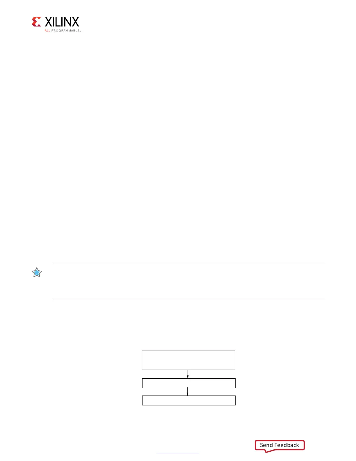
Simulation Debug
Figure 2-49 shows the debug flow for simulation.
X-Ref Target - Figure 2-49
Figure 2-49: Simulation Debug Flowchart
6ERIFY3UCCESSFUL3IMULATION5SING
%XAMPLE$ESIGN)DENTIFYANY)SSUESWITH
3IMULATION%NVIRONMENT
$EBUG)SSUESWITH5SER$ESIGN3IMULATION
/PEN7EB#ASE
 Loading...


