Zynq-7000 AP SoC and 7 Series FPGAs MIS v4.1 616
UG586 November 30, 2016
www.xilinx.com
Chapter 4: LPDDR2 SDRAM Memory Interface Solution
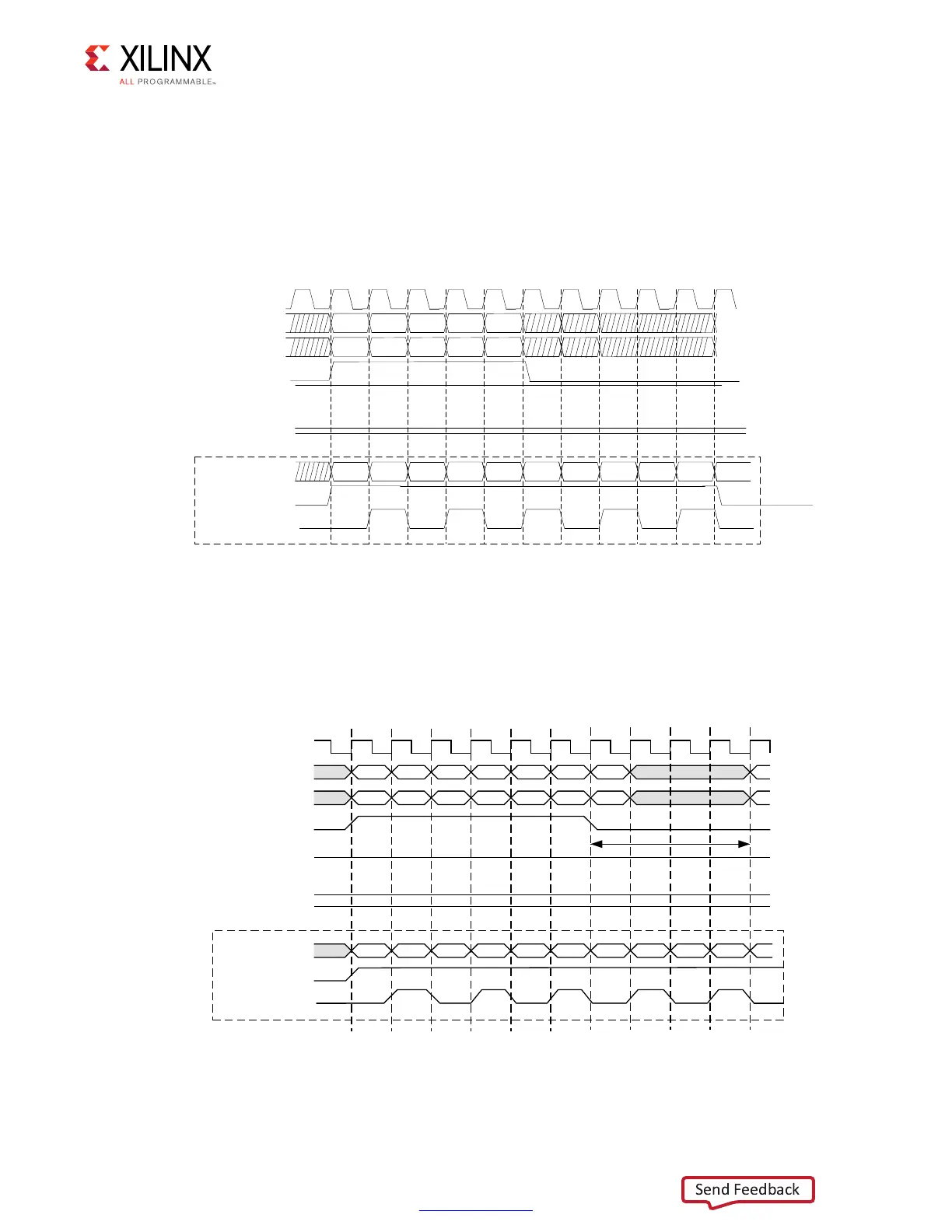
Write Path
The write data is registered in the write FIFO when app_wdf_wren is asserted and
app_wdf_rdy is High (Figure 4-60). If app_wdf_rdy is deasserted, the user logic needs to
hold app_wdf_wren and app_wdf_end High along with the valid app_wdf_data value
until app_wdf_rdy is asserted. The app_wdf_mask signal can be used to mask out the
bytes to write to external memory.
As shown in Figure 4-59, the maximum delay for a single write between the write data and
the associated write command is two clock cycles. When issuing back-to-back write
commands, there is no maximum delay between the write data and the associated
back-to-back write command, as shown in Figure 4-61.
X-Ref Target - Figure 4-60
Figure 4-60: UI Interface Back-to-Back Write Commands Timing Diagram (Memory Burst
Type = BL8)
X-Ref Target - Figure 4-61
Figure 4-61: UI Interface Back-to-Back Write Commands Timing Diagram (Memory Burst
Type = BL8)
FON
DSSBUG\
DSSBZGIBPDVN
DSSBZGIBUG\
DSSBFPG
:5,7(
DSSBDGGU
$GGUD
DSSBHQ
DSSBZGIBZUHQ
DSSBZGIBHQG
DSSBZGIBGDWD
:D :D :E :E :F :F :G
:5,7( :5,7( :5,7( :5,7(
$GGUE $GGUF $GGUG $GGUH
:G :H
:H
DSSBZGIBGDWD
FON
DSSBFPG
:D
:5,7( :5,7( :5,7( :5,7( :5,7( :5,7( :5,7(
DSSBDGGU
$GGUD $GGUE $GGUF $GGUG $GGUH $GGUI $GGUJ
DSSBZGIBHQG
DSSBHQ
DSSBZGIBZUHQ
DSSBUG\
DSSBZGIBPDVN
DSSBZGIBUG\
:D :E :E :F :F :G
:G :H :H
:I
 Loading...


