Zynq-7000 AP SoC and 7 Series FPGAs MIS v4.1 298
UG586 November 30, 2016
www.xilinx.com
Chapter 2: QDR II+ Memory Interface Solution
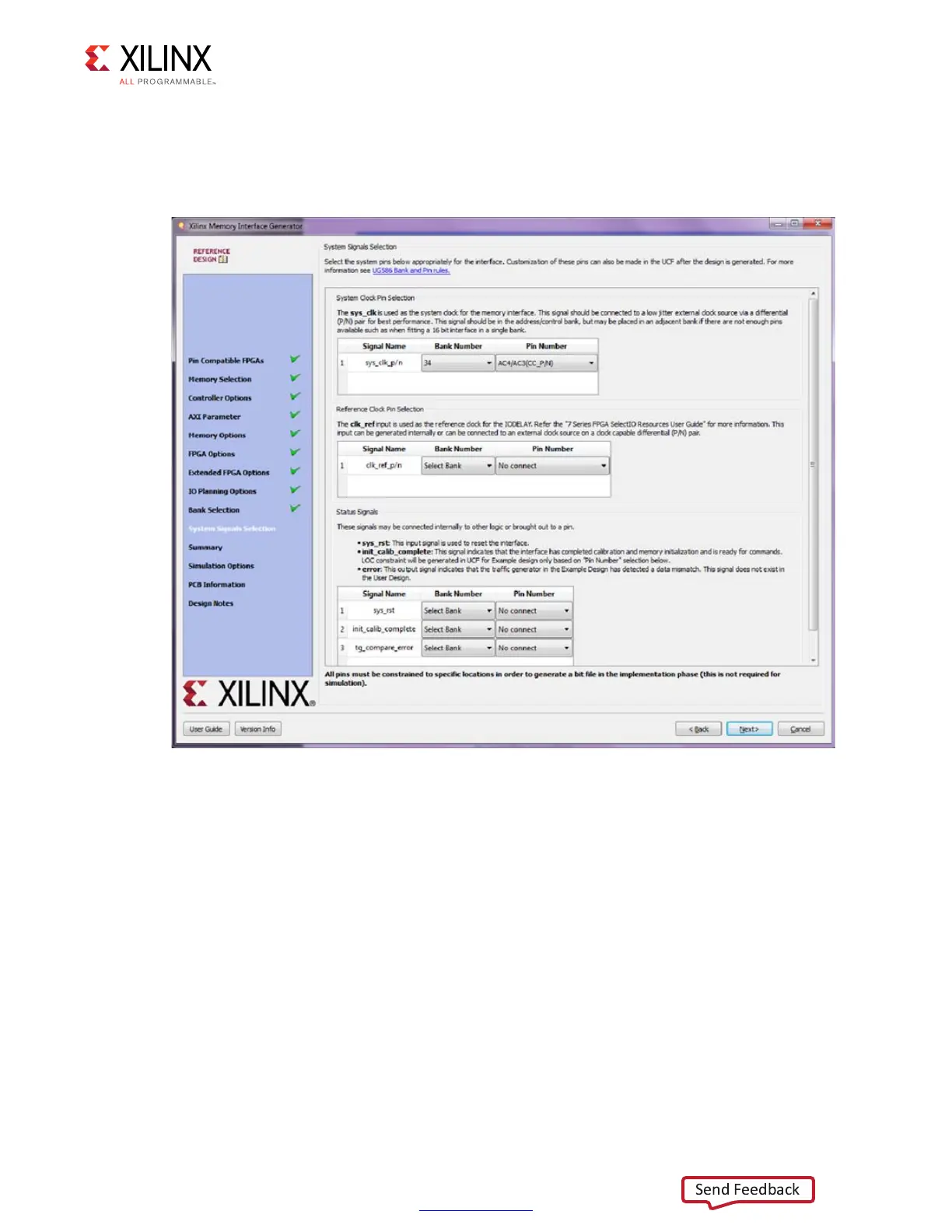
System Pins Selection
Select the pins for the system signals on this page. The MIG tool allows the selection of
either external pins or internal connections, as desired.
• sys_clk – This is the system clock input for the memory interface and is typically
connected to a low-jitter external clock source. Either a single input or a differential
pair can be selected based on the System Clock selection in the FPGA Options page
(Figure 2-21). The sys_clk input must be in the same column as the memory
interface. If this pin is connected in the same banks as the memory interface, the MIG
tool selects an I/O standard compatible with the interface, such as DIFF_HSTL_I or
HSTL_I. If sys_clk is not connected in a memory interface bank, the MIG tool selects
an appropriate standard such as LVCMOS18 or LVDS. The XDC can be modified as
desired after generation.
• clk_ref – This is the reference frequency input for the IDELAY control. This is a 200 MHz
input. The clk_ref input can be generated internally or connected to an external
source. A single input or a differential pair can be selected based on the System Clock
selection in the FPGA Options page (Figure 2-21). The I/O standard is selected in a
similar way as sys_clk above.
X-Ref Target - Figure 2-26
Figure 2-26: System Pins Selection Page
 Loading...


