Zynq-7000 AP SoC and 7 Series FPGAs MIS v4.1 532
UG586 November 30, 2016
www.xilinx.com
Chapter 4: LPDDR2 SDRAM Memory Interface Solution
The desired input clock period is selected from the list. These values are determined by the
memory clock period chosen and the allowable limits of the parameters. For more
information on the MMCM parameter limits, see Design Guidelines, page 631.
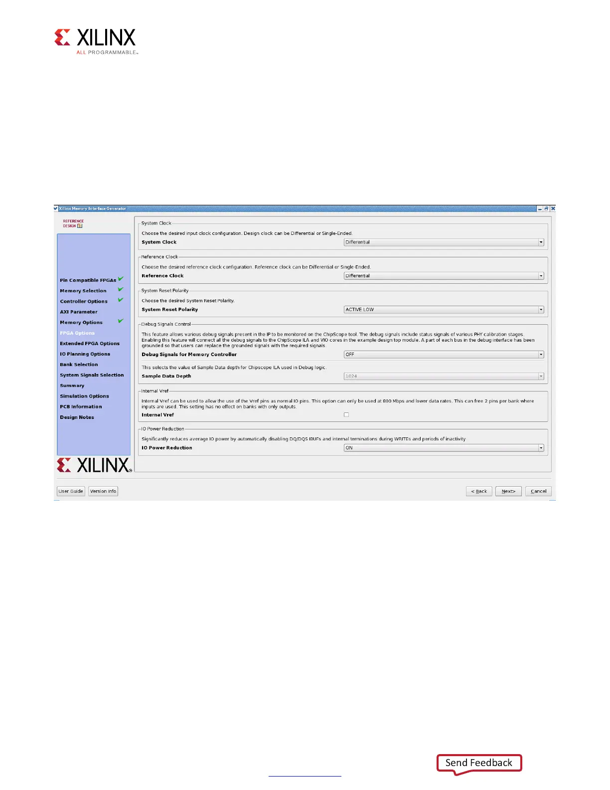
Click Next to display the FPGA Options page.
FPGA Options
Figure 4-21 shows the FPGA Options page.
• System Clock – This option selects the clock type (Single-Ended, Differential, or No
Buffer) for the sys_clk signal pair. When the No Buffer option is selected, IBUF
primitives are not instantiated in RTL code and pins are not allocated for the system
clock.
If the designs generated from MIG for the No Buffer option are implemented without
performing changes, designs can fail in implementation due to IBUFs not instantiated
for the sys_clk_i signal. So for No Buffer scenarios, sys_clk_i signal needs to be
connected to an internal clock.
X-Ref Target - Figure 4-21
Figure 4-21: FPGA Options
 Loading...


