EasyManuals Logo

Xilinx Zynq-7000 User Manual

Xilinx Zynq-7000
678 pages
To Next Page IconTo Next Page
To Previous Page IconTo Previous Page
Page #142 background imageLoading...
Page #142 background image
Zynq-7000 AP SoC and 7 Series FPGAs MIS v4.1 142
UG586 November 30, 2016
www.xilinx.com
Chapter 1: DDR3 and DDR2 SDRAM Memory Interface Solution
Datapath
The datapath comprises the write and read datapaths. The datapath in the 7 series FPGA is
completely implemented in dedicated logic with IN/OUT_FIFOs interfacing the FPGA logic.
The IN/OUT_FIFOs provide datapath serialization/deserialization in addition to clock
domain crossing, thereby allowing the FPGA logic to operate at low frequencies up to 1/4
the frequency of the DDR2 or DDR3 SDRAM clock. Figure 1-60 shows the block diagram of
the datapath.
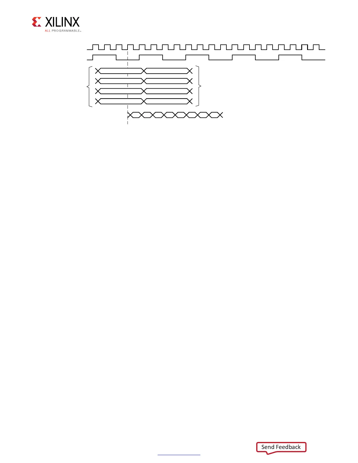
X-Ref Target - Figure 1-59
Figure 1-59: Address/Command Timing Diagram
5'?C??
#,+
#,+$)6
)NPUTSTO/3%2$%3IN3$2
/3%2$%3/UTPUT
#MD #MD
#MD #MD
#MD #MD
#MD

#MD
2!3?.#!3?.7%?.
#3?.!$$2"!
Send Feedback

Table of Contents

Other manuals for Xilinx Zynq-7000

Questions and Answers:

Question and Answer IconNeed help?

Do you have a question about the Xilinx Zynq-7000 and is the answer not in the manual?

Xilinx Zynq-7000 Specifications

General IconGeneral
SeriesZynq-7000
Number of CoresDual-core
Processor SpeedUp to 1 GHz
Device TypeSoC
Logic CellsUp to 350K
DSP SlicesUp to 900
External Memory InterfacesDDR3, DDR2, LPDDR2
I/O StandardsLVCMOS, HSTL, SSTL
Operating Temperature-40°C to +100°C (Industrial), 0°C to +85°C (Commercial)
Package OptionsVarious BGA packages
I/O Voltage3.3V

Related product manuals