Zynq-7000 AP SoC and 7 Series FPGAs MIS v4.1 258
UG586 November 30, 2016
www.xilinx.com
Chapter 1: DDR3 and DDR2 SDRAM Memory Interface Solution
Debugging Read Leveling Failures (dbg_rdlvl_err[0] = 1)
For memory clock frequencies of 400 MHz and above, Read Leveling is performed after
Write Calibration.
Calibration Overview
The final read DQS to read DQ centering is done in this stage of calibration. The first step in
this stage is to decrease the IDELAY and PHASER_IN stage 2 taps values to zero to undo
MPR read leveling. MPR read leveling was only required for OCLKDELAYED calibration. This
stage of read leveling accurately centers the read DQS in the read DQ window using a
993377EECC992244 data pattern. If this stage calibrates successfully, the
init_calib_complete signal is asserted and calibration is complete.
Debug
• If this stage of calibration failed with the assertion of dbg_rdlvl_err[0], set the ILA
trigger to dbg_rdlvl_err[0].
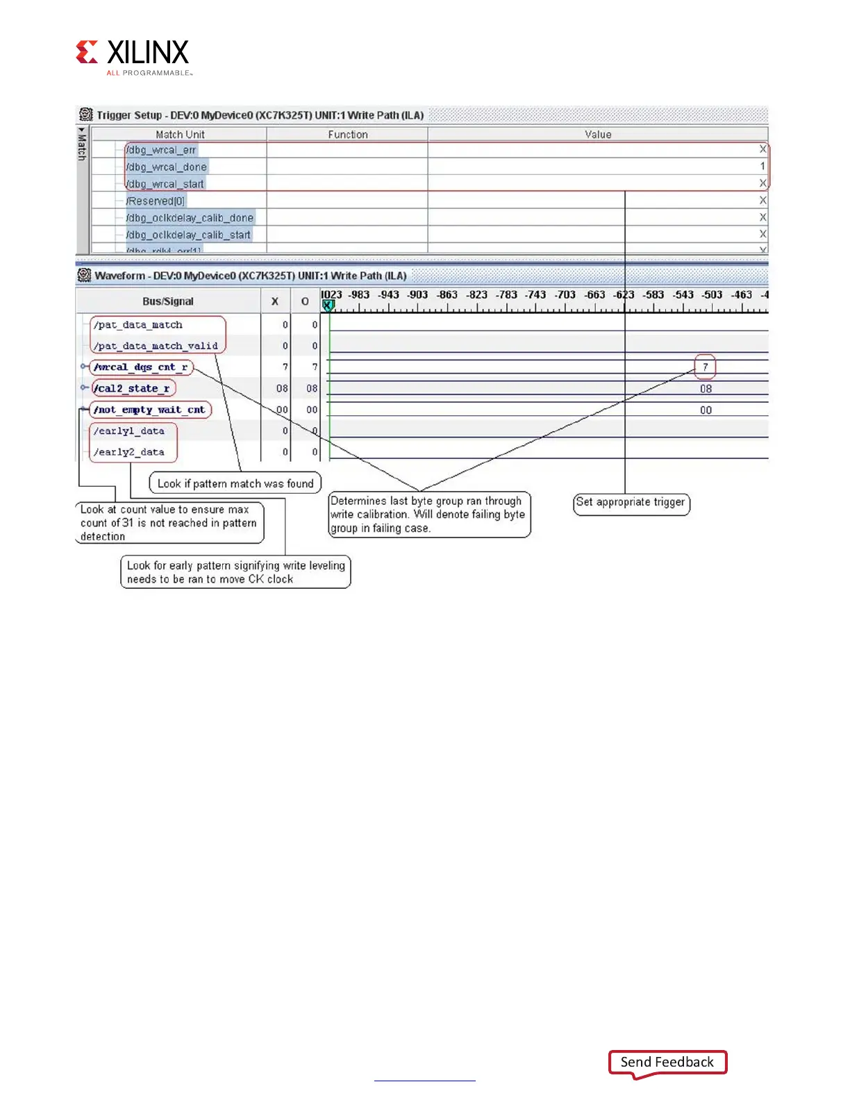
X-Ref Target - Figure 1-104
Figure 1-104: Trigger = dbg_wrcal_done
 Loading...


