Zynq-7000 AP SoC and 7 Series FPGAs MIS v4.1 594
UG586 November 30, 2016
www.xilinx.com
Chapter 4: LPDDR2 SDRAM Memory Interface Solution
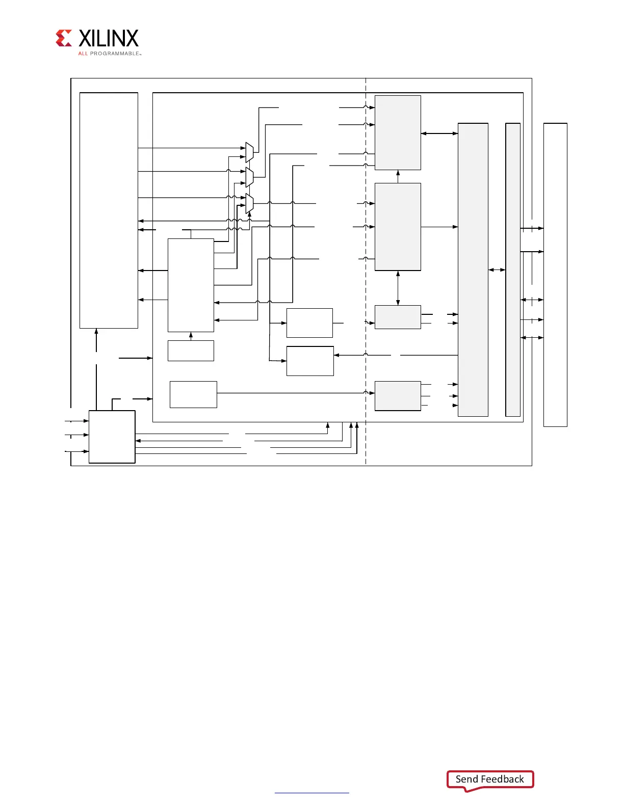
Memory Initialization and Calibration Sequence
After deassertion of system reset, the PHY performs the required power-on initialization
sequence for the memory. This is followed by several stages of timing calibration for both
the write and read datapaths. After calibration is complete, the PHY indicates that
initialization is finished, and the controller can begin issuing commands to the memory.
Figure 4-49 shows the overall flow of memory initialization and the different stages of
calibration.
X-Ref Target - Figure 4-48
Figure 4-48: PHY Block Diagram
I/O FIFOs
PHY Control Block
Phaser_INs
Phaser_OUTs
System
Clock/
Reset
Generation
FREQ_REFCLK
REF_DLL_LOCK
PHY Control Word/
Control Enable
Memory Addr/ Cmd/Control
And
I/O FIFO Enables
IOI
(ISERDES,
OSERDES,
ODDR,
IDELAY)
ICLK1X
ICLKDIV
OCLK1X
OCLKDIV
OCLK1X_90
DQS
FPGA
IOB
LPDDR2
SDRAM
Initialization
And
Calibration
Command
Sequencer
PRBS
Data Pattern
Generator
Mask
(DM)
Strobe
(DQS)
Data
(DQ)
Addr/
Cmd/
Control
Clocks
MEM_REFCLK
System
Clock
System
Reset
IDELAY
REFCLK
Reset
DDR2/DDR3 SDRAM PHY Interface
Addr/
Cmd/
Control/
Write Data
Write Data/Mask
Read leveling stg1
and PRBS
calibration
Phaser_In
Delay
Controls
Read Data
PHY Control Status
I/O FIFO
Status Flags
LPDDR2
Memory
Controller
Initialization
Status
Read
Data
Valid
Read
Data
Offset
Calibration Enable
Sync_In
FABRIC LOGIC
WRLVL off Delayes
PHASE
DETECTOR
Divided by 2 or 4
Of MEM_REFCLK
 Loading...


