Zynq-7000 AP SoC and 7 Series FPGAs MIS v4.1 495
UG586 November 30, 2016
www.xilinx.com
Chapter 3: RLDRAM II and RLDRAM 3 Memory Interface Solutions
Test Bench
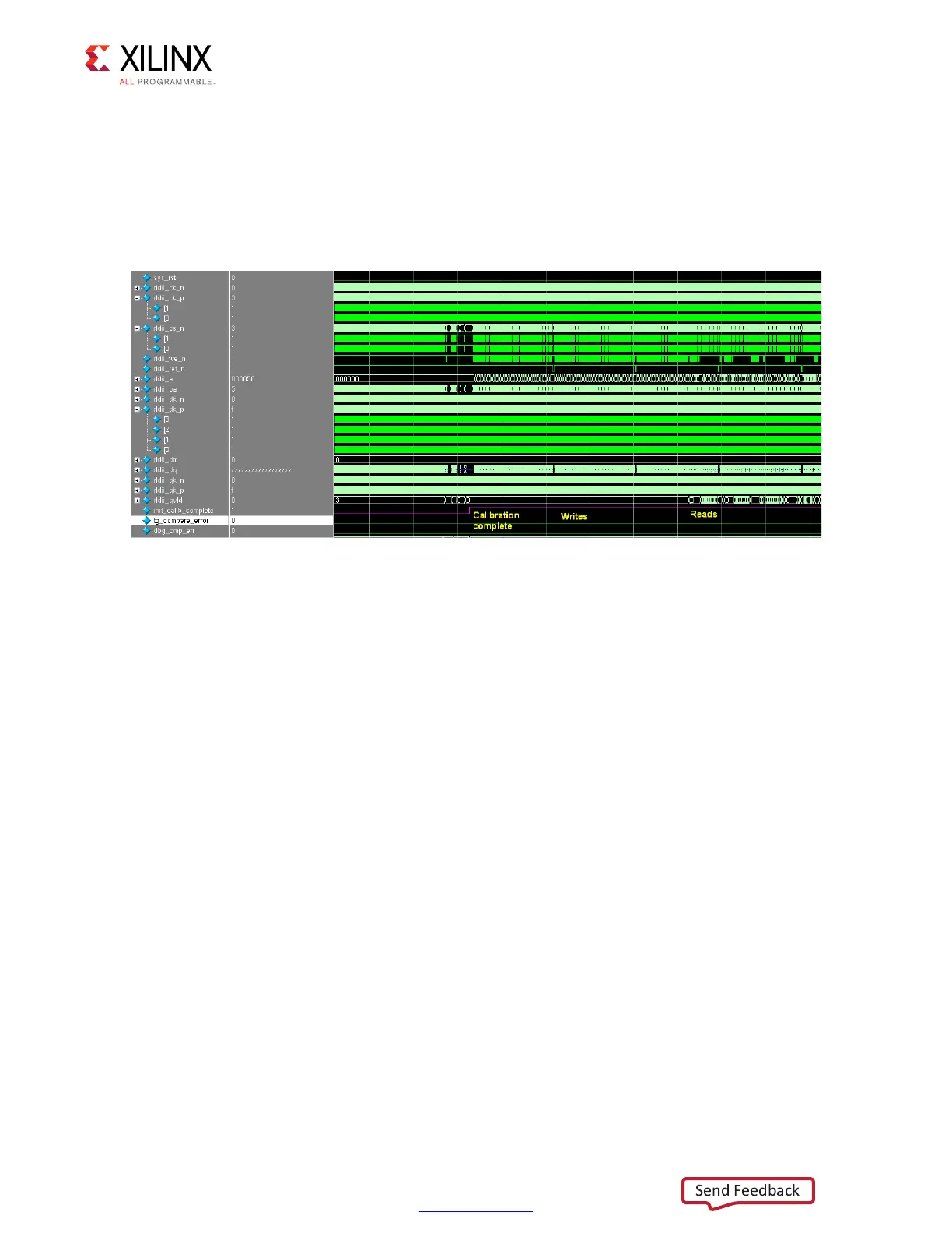
After init_calib_complete is asserted, the test bench takes control, writing to and
reading from the memory. The data written is compared to the data read back. Any
mismatches trigger an assertion of the error signal. Figure 3-73 shows a successful
implementation of the test bench with no assertions on error.
Proper Write and Read Commands
When sending write and read commands, you must properly assert and deassert the
corresponding UI inputs. See Client Interface, page 427 and Interfacing with the Core
through the Client Interface, page 429 for full details. The test bench design provided
within the example design can be used as a further source of proper behavior on the UI.
To debug data errors on the RLDRAM II/RLDRAM 3 interface, it is necessary to pull the UI
signals into the simulation waveform.
In the Questa Advanced Simulator Instance window, highlight u_ip_top to display the
necessary UI signals in the Objects window, as shown in Figure 3-74. Highlight the user
interface signals noted in Table 3-26, page 491, right-click, and select Add > To Wave >
Selected Signals.
X-Ref Target - Figure 3-73
Figure 3-73: Test Bench Operation After Completion of Calibration
 Loading...


