Zynq-7000 AP SoC and 7 Series FPGAs MIS v4.1 109
UG586 November 30, 2016
www.xilinx.com
Chapter 1: DDR3 and DDR2 SDRAM Memory Interface Solution
Table 1-34 describes the register bit usage when DQ_WIDTH = 72.
Table 1-35 describes the register bit usage when DQ_WIDTH = 144.
UE_FFA[31:0]
This register stores the address (Bits[31:0]) of the first occurrence of an access with an
uncorrectable error. When the UE_STATUS bit in the ECC Status register is cleared, this
register is re-enabled to store the address of the next uncorrectable error. Storing of the
failing address is enabled after reset.
UE_FFA[63:32]
Note: This register is unused if C_S_AXI_ADDR_WIDTH < 33.
This register stores the address (Bits[63:32]) of the first occurrence of an access with an
uncorrectable error. When the UE_STATUS bit in the ECC Status register is cleared, this
register is re-enabled to store the address of the next uncorrectable error. Storing of the
failing address is enabled after reset.
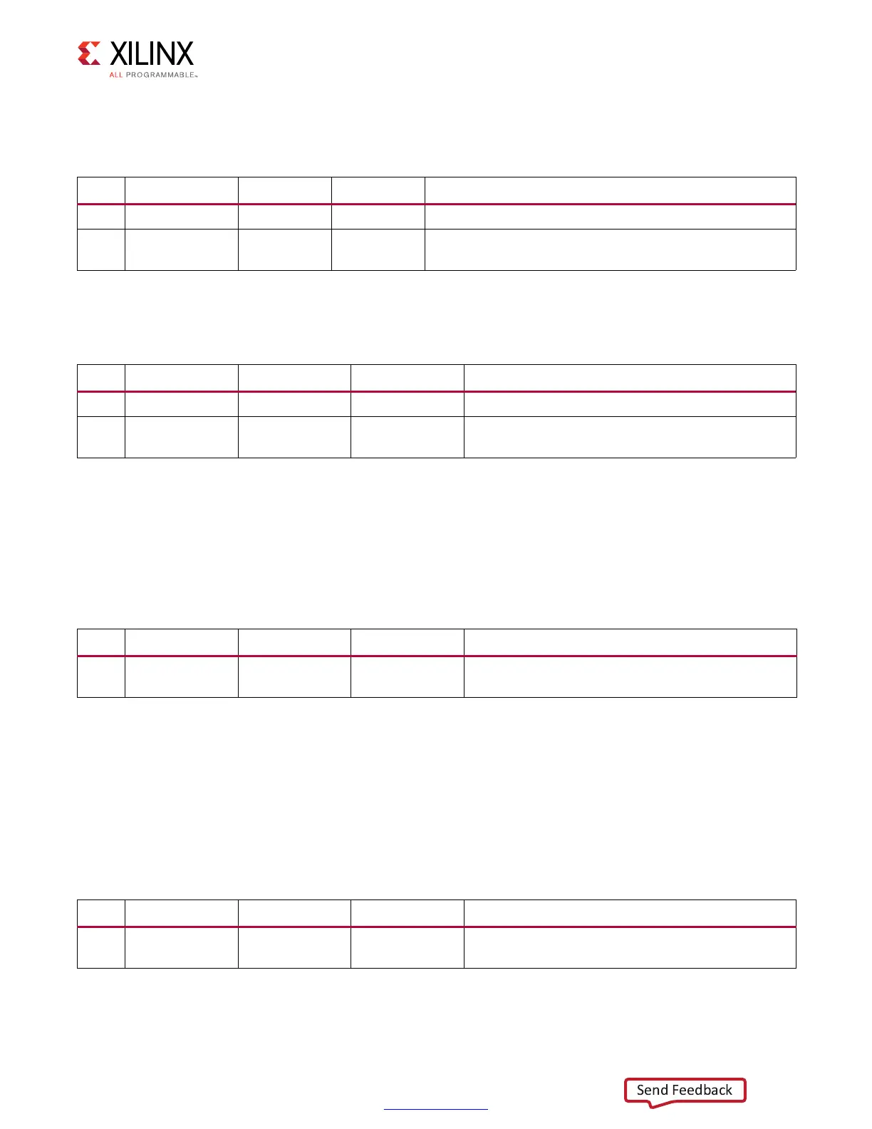
Table 1-34: Correctable Error First Failing ECC Register Bit Definitions for 72-Bit External Memory
Width
Bits Name Core Access Reset Value Description
31:8 Reserved RSVD – Reserved
7:0 CE_FFE R 0
ECC (Bits[7:0]) of the first occurrence of a correctable
error.
Table 1-35: Correctable Error First Failing ECC Register Bit Definitions for 144-Bit External Memory
Width
Bits Name Core Access Reset Value Description
31:16 Reserved RSVD – Reserved
15:0 CE_FFE R 0
ECC (Bits[15:0]) of the first occurrence of a
correctable error.
Table 1-36: Uncorrectable Error First Failing Address [31:0] Register Bit Definitions
Bits Name Core Access Reset Value Description
31:0 UE_FFA [31:0] R 0
Address (Bits[31:0]) of the first occurrence of an
uncorrectable error.
Table 1-37: Uncorrectable Error First Failing Address [31:0] Register Bit Definitions
Bits Name Core Access Reset Value Description
31:0 UE_FFA[63:32] R 0
Address (Bits[63:32]) of the first occurrence of an
uncorrectable error
 Loading...


