Zynq-7000 AP SoC and 7 Series FPGAs MIS v4.1 361
UG586 November 30, 2016
www.xilinx.com
Chapter 2: QDR II+ Memory Interface Solution
For detailed information on setting up Xilinx libraries, see COMPXLIB in the Command Line
Tools User Guide (UG628) [Ref 17] and the Synthesis and Simulation Design Guide (UG626)
[Ref 18]. For simulator tool support, see the Zynq-7000 AP SoC and 7 Series Devices Memory
Interface Solutions Data Sheet (DS176) [Ref 1].
A working example design simulation completes memory initialization and runs traffic in
response to the test bench stimulus. Successful completion of memory initialization and
calibration results in the assertion of the cal_done signal. When this signal is asserted, the
Traffic Generator takes control and begins executing writes and reads according to its
parameterization.
Table 2-15 shows the signals and parameters of interest, respectively, during simulation.
Memory Initialization
The QDR II+ memories do not require an elaborate initialization procedure. However, you
must ensure that the Doff_n signal is provided to the memory as required by the vendor.
The QDR II+ SRAM interface design provided by the MIG tool drives the Doff_n signal
from the FPGA. After the internal MMCM has locked after a wait period of 200 μs, the
Doff_n signal is asserted High. After Doff_n is asserted and following CLK_STABLE (set to
2,048) number of CQ clock cycles, commands are issued to the memory.
For memory devices that require the Doff_n signal to be terminated at the memory and
not be driven from the FPGA, you must perform the required termination procedure.
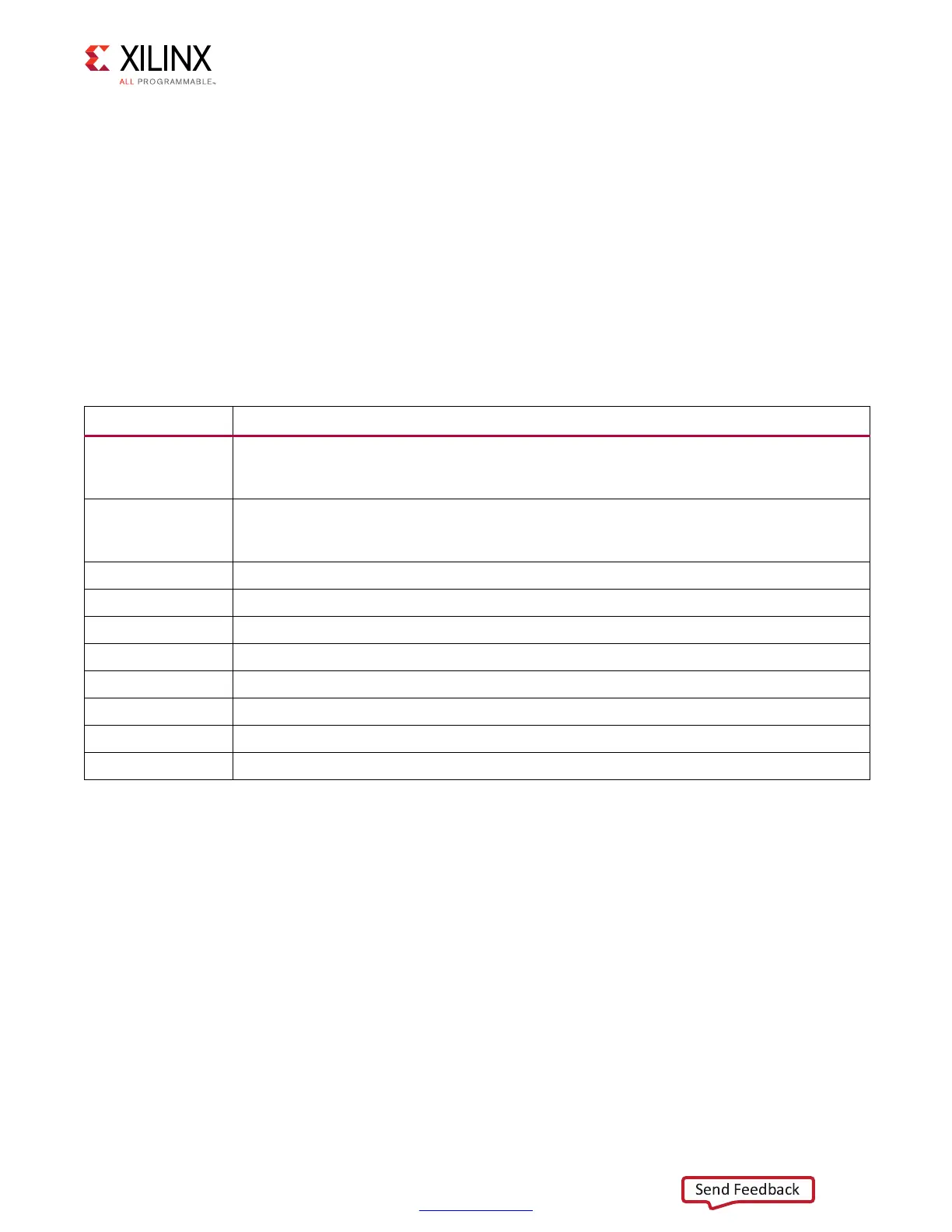
Table 2-15: Signals of Interest During Simulation
Signal Name Usage Description
tg_compare_error
This signal indicates a mismatch between the data written from the UI and data received
during a read on the UI. This signal is a part of the example design. A single error asserts
this signal; it is held until the design is reset.
tg_cmp_error
This signal indicates a mismatch between the data written from the UI and the data received
during a read on the UI. This signal is part of the example design. This signal is asserted
each time a data mismatch occurs.
app_wr_cmd This signal indicates that the write address and write data are valid for a write command
app_wr_addr This is the address provided for the write command
app_wr_data This is the write data for a write command
app_wr_bw_n This signal is the byte write control
app_rd_cmd This signal indicates that the read address is valid for a read command
app_rd_addr This address is provided for the read command
app_rd_data This read data is returned from the memory device
app_rd_valid This signal is asserted when app_rd_data is valid
 Loading...


